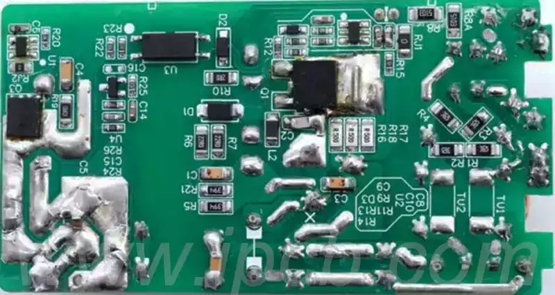
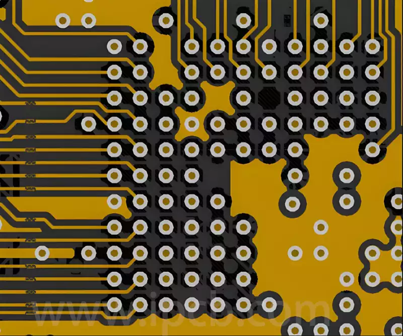
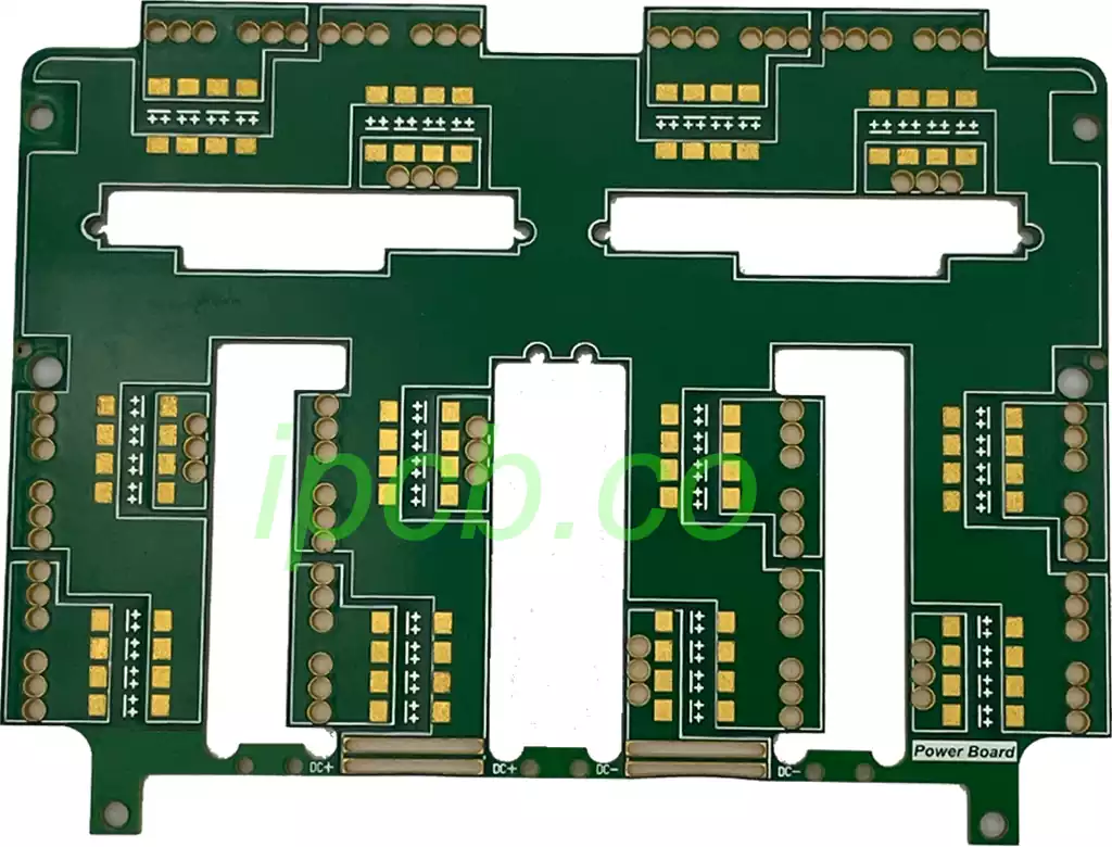
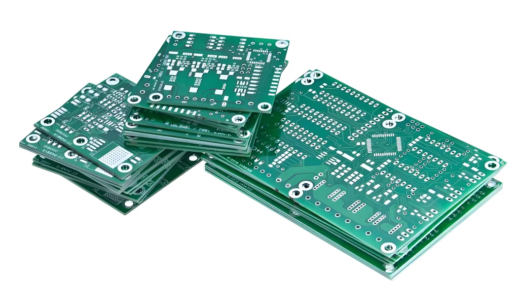
In the grand technological landscape of modern human civilization, from the palm-touch smart mobile terminals and self-driving cars navigating city traffic to satellite communication payloads exploring deep space, almost all electronic devices embodying the crystallization of human wisdom conceal an incredibly precise microscopic electronic world. If we liken a printed circuit board (PCB) to the blueprint and road infrastructure of this microscopic city, then the core process of firmly fixing and giving life to various active chips, passive components, and connectors through metallurgy and fluid mechanics is Printed Circuit Assembly (PCBA).
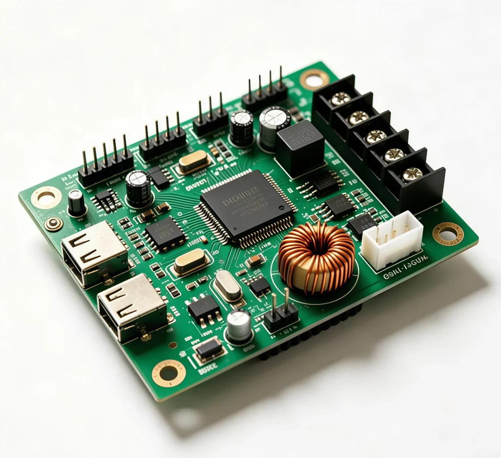
PCBA is far more than simply “gluing” components onto a circuit board. It is a highly intensive interdisciplinary systems engineering project, perfectly integrating polymer chemistry, precision mechanical fluid dynamics, thermodynamics, micro-metallurgy, and modern automation control. From an isolated roll of solder paste and a tiny surface-mount capacitor almost invisible to the naked eye to ultimately becoming a fully functional high-end electronic computing unit, this process bridges a manufacturing chasm filled with both physical challenges and engineering ingenuity.
This article will meticulously analyze and progressively explore the physical essence, core process rheology, thermodynamic bonding mechanisms, and rigorous quality verification engineering of the entire lifecycle of printed circuit board (PCB) assembly.
From Bare Board to Active System: The Physical Essence and System Positioning of PCBA
To understand the greatness of PCB assembly, we must first clarify the qualitative leap between PCB and PCBA.
A bare PCB, fresh from the etching workshop, may possess intricate conductive copper traces, insulating solder mask layers, and precise micron-level blind and buried vias, but it is essentially still a “dead” circuit board. It lacks any capabilities for logic operations, signal amplification, energy conversion, or data storage. It’s like an empty city with decoupling roads and overpasses, lacking citizens and vehicles bustling about.
Printed circuit board assembly (PCBA) is the assembly process that breathes life into this empty city.
In the microscopic world of a PCBA (Precast Concrete Analog Board), all electronic components play different social roles:
Semiconductor integrated circuit chips are like the central brain and decision-making nerve center of a skyscraper, processing massive amounts of digital and analog signals;
Resistors and capacitors are like voltage regulators and damping valves at various nodes in a city, silently maintaining the stability of current and voltage;
Inductors and transformers are like substations and magnetic field energy buffers, ensuring the flawless operation of the entire power distribution network;
Connectors and interface components act as transportation hubs to the external physical world, continuously inputting energy and outputting data.
The core goal of PCBA manufacturing engineering is to integrate these physical entities with vastly different characteristics and materials within micrometer-level spatial precision, through reliable mechanical support and low-resistance, high-strength metallurgical electrical interconnections, into a high-density electromagnetic system capable of long-term stable operation.
Precision Fluid Dynamics Exercise: Solder Paste Printing and Stencils
The first physical process in the entire PCBA manufacturing process often determines more than 70% of the final soldering yield of the entire board. This is solder paste printing.
The Rheological Nature of Solder Paste
Solder paste is not ordinary glue, but a microscopic composite fluid with an extremely complex composition. It is made by uniformly mixing and stirring fine metal alloy powders (traditionally tin-lead alloys, but nowadays the mainstream is environmentally friendly tin-silver-copper lead-free alloy powders) with a high-viscosity organic flux. The metal powders typically appear as highly regular micron-sized spheres, suspended in a flux matrix with thixotropic properties.
The flux plays multiple physicochemical roles: it must exhibit good thixotropy during printing—that is, its viscosity must drop sharply under squeegee shear force, flowing smoothly like a liquid; and the viscosity must recover rapidly within milliseconds the moment the shear force disappears, maintaining a perfect three-dimensional shape without collapse or sagging. Simultaneously, the activating components in the flux also bear the responsibility of removing the microscopic oxide film on the surface of the copper pads during soldering.
Stencil Apertures and Fluid Transfer Efficiency
To accurately print thousands of tiny solder paste blobs onto corresponding pads on a circuit board, a high-precision metal stencil is essential.
The stencil is typically made of a thin sheet of high-strength stainless steel, with micro-holes precisely corresponding to the circuit board pads created using laser cutting technology. On the printing press, the circuit board and stencil are tightly bonded, and a squeegee pushes the solder paste across the stencil at a constant speed, angle, and pressure.
In this process, the principles of fluid dynamics are clearly demonstrated. The pressure of the squeegee pushing forward forces the solder paste into the micro-holes of the stencil, directly contacting the exposed copper pads of the circuit board below. At the moment the squeegee passes and the stencil separates perpendicularly from the circuit board, a microscopic tug-of-war unfolds between the physical “peeling force” and the “wetting adhesion force” of the solder paste to the copper pads. To ensure 100% solder paste detaches from the stencil and remains perfectly on the pads, the roughness of the stencil walls must be controlled at the nanometer level. Electrochemical polishing after laser cutting is even necessary to create tiny tapered openings, minimizing resistance during demolding.
Any minute printing defect—such as insufficient solder paste leading to cold solder joints, excessive solder paste causing bridging and short circuits, or stencil residue causing spikes—will be magnified exponentially during subsequent soldering heat treatment, becoming a potential hardware failure.
High-speed automation and micron-level spatial alignment: Surface Mount Technology (SMT)
When the circuit board with a perfectly patterned solder paste emerges from the printer, it immediately enters the most technologically advanced and impressive workshop in the entire PCBA manufacturing process—the Surface Mount Technology (SMT) high-speed placement production line.
Visual recognition and optical spatial coordinate system: Modern fully automated high-speed placement machines represent the pinnacle of human precision mechanical manufacturing. Faced with microchips measuring only one millimeter square, or even those employing Ball Grid Array (BGA) packages with hundreds of concealed pins, robotic arms cannot grasp them by sight or rigid mechanical coordinates.
Once the circuit board enters the pick-and-place machine’s track and is secured by vacuum fixtures, the machine first uses its onboard high-resolution vision camera to rapidly scan the optical positioning points (mark points) along the circuit board’s edge. These geometric patterns, composed of exposed immersion gold copper, serve as the physical spatial origin of the entire board. Through image distortion correction and 3D matrix calculations of these mark points, the pick-and-place machine’s central processing unit can instantly establish a dynamic physical coordinate system with micron-level precision, accurately eliminating the minute thermal expansion and contraction and physical deflections that occur during the board’s movement.
High-speed nozzles and dynamic inertial control: Inside the pick-and-place machine, rotary or multi-module linearly driven placement heads move back and forth between the feeder and the circuit board at dazzling speeds.
The feeder, like a row of neatly arranged magnetic tape drives, continuously dispenses miniature electronic components encapsulated in paper or plastic tape. A miniature vacuum nozzle at the bottom of the placement head instantly picks up the component. As it flies towards the circuit board, an upward-looking camera (Laser/Vision Centering) above the nozzle captures the component’s spatial projection under vacuum. Complex algorithms calculate the component’s center deviation and rotation angle, and a high-precision servo motor performs millisecond-level rotational corrections during rapid movement.
When the placement head descends and precisely “presses” the component into the moist solder paste on the pads, not only must the absolute coordinate position be controlled, but also the vertical downward pressing depth (Impact Force) must be precisely controlled. If the pressing is too shallow, the component leads will not make sufficient contact with the solder paste; if the pressing is too deep, the solder paste will be squeezed outwards, causing short circuits between adjacent pads. This perfect control of micrometer-level spatial orientation during high-speed movement is the foundation of modern high-density electronics manufacturing.
Thermodynamic Symphony and Metallurgical Bonding: The Physical Evolution of Reflow Soldering Ovens
After the high-precision physical placement of components, the thousands of components on the circuit board are merely temporarily “floating” on the moist solder paste, unable to withstand even the slightest movement. To permanently fix them and establish robust electrical connections, the circuit board must enter the core energy hub of the entire SMT production line—the reflow soldering oven.
Thermodynamic Evolution of Four Temperature Zones The reflow oven is a closed thermodynamic tunnel several meters long, divided into dozens of independently temperature-controlled zones. Driven by a conveyor belt, the circuit board sequentially undergoes four strictly defined physical heat treatment stages:
Preheat Zone: As the circuit board enters the oven, the temperature rises gradually. The core physical purpose of this stage is to slowly evaporate the low-boiling-point volatiles in the organic solvent of the solder paste, preventing the solvent from boiling instantly and generating violent bubbles that could “explode” the newly placed micro-components or create numerous voids within the solder joints. Simultaneously, gentle heating evenly releases the thermal stress within the entire large-area circuit board.
Thermal Soak Zone: The temperature remains at a relatively stable plateau. During this period, the chemical activators in the flux are fully activated, beginning to peel away and reduce metal oxides on the copper pads and component leads, exposing a pure metal atomic substrate. Simultaneously, this zone ensures that the temperature of large components (such as large inductors and transformers) and small components (such as small resistors) on the entire circuit board tends to be consistent, eliminating temperature differences caused by variations in heat capacity.
Reflow Zone: The temperature rapidly breaks through the eutectic melting point of the alloy solder (typically around 217 degrees Celsius for lead-free tin-silver-copper alloys). In the peak temperature range (typically reaching 245 to 260 degrees Celsius), the fine alloy powder in the solder paste completely melts, transforming from a solid state into a liquid metal with extremely high surface tension.
Cooling Zone: After leaving the peak temperature zone, the circuit board rapidly enters the strong cooling section. The liquid alloy crystallizes and solidifies within seconds, returning to a solid metal state, completing the entire soldering process. Interfacial Metallurgy and the Birth of Intermetallic Compounds (IMCs)
In the instant of high-temperature melting in the reflow zone, an invisible microscopic metallurgical miracle is taking place.
Liquid tin atoms, with their extremely high surface activity, rapidly wet the surface of the copper pads and diffuse into the copper lattice. Simultaneously, copper atoms also penetrate into the liquid tin. At the interface between the two, tin and copper combine to grow an extremely thin but crucial microcrystalline structure—the intermetallic compound (IMC).
This IMC layer is neither pure copper nor pure tin, but rather a special alloy phase such as three copper-one tin or six copper-five tin. It acts as the “molecular-level cement” connecting component leads to the copper pads on the circuit board. If the reflow soldering temperature is insufficient or the time is too short, the IMC layer cannot grow sufficiently, resulting in extremely weak mechanical bonding at the solder joints, which will detach even with slight vibration (manifesting as cold solder joints or poor solder joints). Conversely, if the reflow time is too long, the IMC layer becomes excessively thick. This structure, due to its extremely high lattice rigidity, becomes extremely brittle and prone to brittle fracture during long-term thermal expansion and contraction cycles. Therefore, precise control of the reflow oven temperature profile is essentially a precise control of the microscopic metallurgical growth kinetics.
The Adherence to Traditional Hardcore Physics: Through-Hole Technology (THT) and Wave Soldering
Although surface mount technology (SMT) accounts for over 90% of modern electronic manufacturing, traditional through-hole technology (THT) remains irreplaceable when handling industrial, automotive, and high-voltage power components that require resistance to enormous mechanical pulling forces, high current surges, or frequent insertion and removal.
Unlike SMT components, which rely solely on surface pads, THT components have robust metal leads that must pass directly through pre-drilled and metallized vias on the circuit board.
After manual or automated insertion, these circuit boards undergo a completely different soldering process—a wave soldering machine.
In the molten solder bath at the bottom of the wave soldering oven, a mechanical pump forcefully propels high-temperature molten solder upwards, forming a stable, swirling “molten solder wave” through a narrow nozzle. As the circuit board, with its long leads at the bottom, smoothly glides across the solder wave at a certain angle, flux is first sprayed to clean it, and then the copper via walls and protruding leads are completely enveloped by the high-temperature solder wave. Utilizing the natural capillary action within the metallized vias, the molten solder is rapidly drawn upwards into the vias, filling the entire cavity. After the circuit board cools and leaves the solder wave, full, robust, conical through-hole solder joints are formed on the back of the circuit board. This dual protection of physical and mechanical anchoring and metallurgical welding endows THT components with unparalleled resistance to mechanical vibration and tensile strength.
Rigorous Quality Inspection: Automated Optical and X-Ray Non-Destructive Testing Engineering
PCBA boards that have completed all soldering processes must never be directly packaged and shipped. In the complex process of physical and chemical changes, any slight disturbance can introduce hidden dangers. Modern PCBA manufacturing has established a multi-dimensional and rigorous quality verification system.
Automated Optical Inspection (AOI) and Solder Paste Inspection (SPI)
At critical points, the Automated Optical Inspection (AOI) system acts like a tireless judge. High-definition industrial cameras, combined with multi-angle color LED light sources, perform a comprehensive scan of each board. AOI can identify missing components, incorrect components, reversed polarity (e.g., electrolytic capacitors reversed positive and negative), misalignment, and obvious bridging short circuits and insufficient solder defects with extremely high precision. Solder paste inspection (SPI) following the printing process utilizes laser 3D contour scanning to intercept, clean, and reprint substandard solder paste prints with insufficient thickness or volume misalignment before components are attached, eliminating defects at the outset.
X-Ray 3D Tomographic Scanning and Hidden Solder Joint Insight
However, with the widespread adoption of bottom-leadless chip packages such as BGA (Ball Grid Array), traditional visible light AOI has become completely ineffective. This is because all the solder balls are directly beneath the chip body, making it impossible for the naked eye or camera to directly observe the morphology of the internal solder joints.
This is where the X-Ray 3D non-destructive testing system comes in.
High-energy X-rays penetrate the entire chip and circuit board, generating a 3D density perspective view of the internal solder joints based on the differences in X-ray absorption rates of materials with different densities. Reconstructed using computed tomography (CT), engineers can clearly “cut open” and observe each tiny solder ball hidden beneath the chip. The core mission of X-Ray is to identify hidden solder voids. If flux gas is not properly vented during reflow soldering, air bubbles will remain inside the solder balls. Excessively large voids severely reduce the current-carrying cross-sectional area of the solder joint, causing localized current density surges, overheating, and burnout. Only through rigorous X-Ray testing can the density and perfection of each hidden solder joint be ensured.
In-Circuit Testing (ICT) and Functional Testing (FCT)
Finally, the ultimate test of electrical performance.
In-Circuit Testing (ICT) utilizes spring-loaded probes (pogo pins) spread across a specialized bed of pins to precisely contact hundreds or thousands of test pads on the back of the circuit board. By applying minute test voltages and currents, it instantly detects the actual capacitance and resistance values of each resistor, capacitor, and diode, identifying open and short circuits. Functional Testing (FCT), on the other hand, connects the entire PCBA to a fixture simulating its real-world operating environment, powers it on, and runs the actual firmware program, performing a comprehensive dynamic evaluation of its RF transmit power, communication protocol handshake, and input/output response. Only PCBAs that pass these rigorous tests are eligible to be labeled as qualified and used in the real world.
In summary
Printed Circuit Assembly (PCB) is a silent symphony in modern technology industry. It perfectly intertwines abstract digital logic code with macroscopic physical entities through precise fluid printing, high-speed mechanical positioning, high-temperature metallurgical thermal bonding, and stringent optical and electrical testing.
Within this tiny microscopic world, every molecular-level crystal growth and every nanoscale spatial alignment silently propels human society toward a future of higher speed, lower power consumption, and greater reliability. Understanding the manufacturing engineering and physical essence of PCBAs is not only about mastering an electronics manufacturing technology, but also about glimpsing the core of the precision and magnificence of modern human cutting-edge industrial civilization.