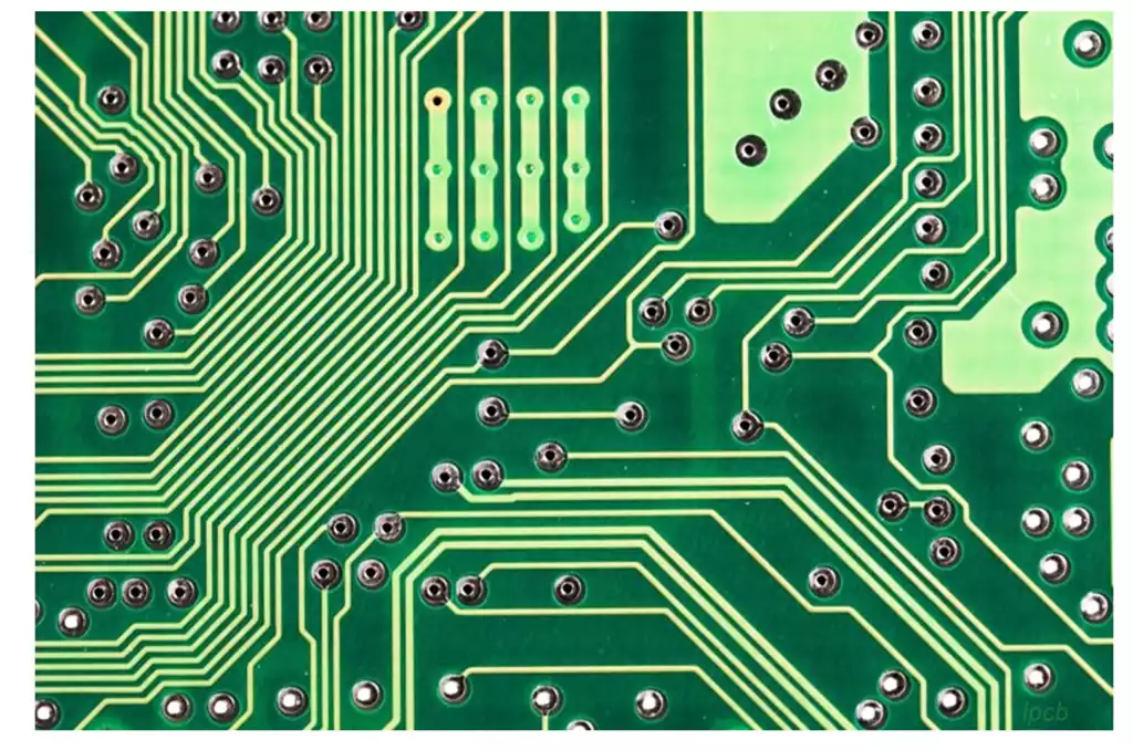
What are HDI printed circuit boards, and why are they used instead of conventional multilayer PCBs? HDI stands for High Density Interconnect. An HDI PCB uses microvias, fine conductors, small capture pads and sequentially added dielectric layers to place more electrical connections within a limited board area.
The difference is not simply that an HDI board has many components. When engineers ask what are HDI printed circuit boards, the more useful answer lies in how the layers are connected. Conventional mechanically drilled holes may pass through the complete board, while laser-drilled microvias create short connections between selected adjacent layers.
This structure allows routing to continue beneath fine-pitch BGA and CSP packages without allowing large through-holes and clearance areas to occupy every layer.
What Makes a PCB an HDI Board
An ordinary multilayer PCB can have a high component count without using HDI construction. What distinguishes an HDI PCB is the combination of reduced interconnection geometry and build-up manufacturing.
A typical structure contains a conventional multilayer core surrounded by one or more thin dielectric and copper layers. Laser-drilled microvias connect these outer build-up layers. Buried vias may connect layers inside the core, while plated through-holes can still be used where a connection must pass through the complete board.
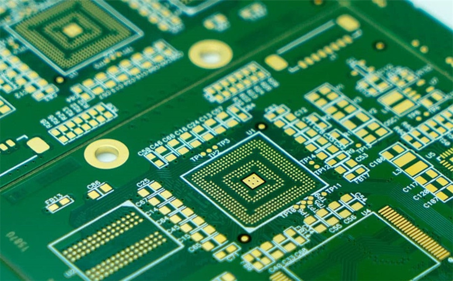
Therefore, the answer to what are HDI printed circuit boards is not based only on the number of layers. A six-layer board with microvias and sequential lamination may use more advanced HDI technology than a conventional twelve-layer board containing only mechanically drilled through-holes.
IPC documentation identifies microvias as a central characteristic of HDI construction. IPC material specifications have historically described them as small blind or buried connections no larger than 0.15 mm in diameter, although actual manufacturing capability and applicable standards must be confirmed for each project.
Microvias Create Space for Fine Pitch Components
A mechanically drilled through-hole requires a drill diameter, copper plating, an annular ring and clearance from nearby conductors. It also occupies space on every layer through which it passes, even when the electrical connection is needed on only two layers.
A microvia is normally formed by laser drilling through a thin dielectric layer. After cleaning and metallization, it produces a short electrical connection between adjacent copper layers. Because its diameter and capture pad are smaller, more routing channels can pass between or around the pads.
This is particularly useful beneath fine-pitch BGAs. Microvias can be placed inside component pads and filled with copper, allowing signals to move from the surface into an internal routing layer without requiring a large via beside every pad.
For designers researching what are HDI printed circuit boards, via-in-pad is often the most visible feature. However, a microvia should not be placed in a solder pad without considering filling and planarization. An open or uneven via can draw solder away from the component joint and create an unreliable assembly surface.
How HDI Build Up Structures Are Classified
HDI constructions are often described using expressions such as 1+N+1, 2+N+2 and 3+N+3.
In a 1+N+1 structure, N represents the conventionally manufactured multilayer core. One build-up layer is added to each side of that core. A 2+N+2 structure has two sequentially formed HDI layers on each side, while a 3+N+3 structure has three.
Each additional build-up cycle normally requires another sequence of dielectric lamination, laser drilling, via metallization and circuit formation. More cycles can increase routing flexibility, but they also add cost, processing time and registration risk.
Microvias in successive layers may be staggered or stacked. Staggered microvias are offset from one another, allowing each via to land on a separate pad. Stacked microvias are positioned vertically above one another and generally require controlled copper filling to support the next connection.
Understanding this stack-up terminology is essential when answering what are HDI printed circuit boards because two boards described simply as HDI can have substantially different manufacturing difficulty.
Why HDI Increases Routing Density
Fine-pitch packages create a routing problem before they create a board-size problem. A processor may contain hundreds or thousands of terminals, but the available space between its pads is too narrow for conventional traces and through-hole vias.
HDI technology reduces the size of the interconnection structures that compete with those traces. Smaller microvia pads create additional escape-routing channels, while finer lines and spaces allow more conductors to pass through each routing layer.
As a result, an HDI PCB may accomplish the required interconnection with a smaller outline or fewer total layers than a conventional design. This does not mean HDI automatically reduces cost. Savings occur only when the reduced size, layer count or assembly complexity offsets the additional build-up processes.
The practical answer to what are HDI printed circuit boards is therefore connected to routing efficiency. Their purpose is to use the available PCB area more effectively rather than simply making every feature smaller.
Manufacturing Requires Sequential Processing
A conventional multilayer PCB is laminated and then mechanically drilled as a largely complete structure. An HDI board may pass through several controlled build-up cycles.
The process begins with the inner core, which may already contain buried vias. A thin dielectric layer and copper foil are laminated onto the core. Microvias are laser drilled, cleaned and metallized. The copper pattern is formed, and the sequence is repeated if the stack-up requires another build-up layer.
This is why the HDI construction must be finalized before fabrication begins. Changing a microvia from staggered to stacked, increasing its depth or moving it across several dielectric layers can change the manufacturing process rather than merely changing the artwork.
For anyone asking what are HDI printed circuit boards from a manufacturing perspective, they are sequentially constructed interconnect systems. The registration, drilling, plating and lamination results from one stage become the foundation for the next.
Microvia Reliability Depends on Structure and Process
Microvias are short, but their small dimensions leave little room for process variation. Incomplete laser cleaning, poor target-pad preparation or uneven copper deposition can weaken the interface between the microvia and its landing pad.
Stacked microvias create additional concern because several plated interfaces are positioned in the same vertical structure. Reflow cycles and service-temperature changes place mechanical stress on those interfaces.
IPC has previously warned that some microvia interface failures may not be detected through conventional visual inspection and microsection evaluation alone. Appropriate qualification can therefore include resistance measurements, reflow simulation, thermal cycling and test coupons representing the production structure.
This reliability issue is an important part of understanding what are HDI printed circuit boards. HDI does not automatically mean higher reliability. It provides greater interconnection density, but the microvia construction must be designed, fabricated and tested for the expected thermal and mechanical environment.
HDI Can Improve Electrical Performance
Short microvias can reduce the electrical stub associated with a long plated through-hole. Shorter connections may reduce parasitic inductance and capacitance, which can help high-speed signal and power-distribution performance.
The final result still depends on the complete stack-up. Trace geometry, reference-plane continuity, dielectric properties, copper roughness and return paths must remain controlled. Using microvias cannot compensate for poor impedance planning or broken reference planes.
For high-frequency products, the HDI structure should be evaluated as part of the signal path rather than treated only as a way to fit more components onto the board.
When Should HDI Be Used
HDI becomes appropriate when conventional vias and routing rules prevent practical breakout from fine-pitch packages, force an excessive layer count or make the required product dimensions impossible.
Common applications include smartphones, compact industrial controllers, medical electronics, cameras, communication modules, automotive electronics and high-performance computing hardware. The technology is especially valuable where small size, high I/O density and short interconnections are required simultaneously.
It may not be justified for a low-density control board with large components and generous enclosure space. In that case, conventional multilayer construction can provide a simpler and more economical solution.
Before selecting the structure, buyers should provide the PCB manufacturer with the proposed stack-up, BGA pitch, minimum line width and spacing, microvia diameter, via arrangement, copper thickness, impedance requirements and expected reliability class.
For an HDI project entering production, iPCB can review the microvia structure, sequential lamination requirements, material selection and inspection plan before fabrication. Early review is particularly important when stacked microvias or multiple build-up cycles are involved.
HDI Is a Manufacturing Architecture
So what are HDI printed circuit boards in practical terms? They are PCBs that combine microvias, fine conductor geometry and sequential build-up layers to create more routing connections within a smaller area.
Their main advantage is not simply a higher component count. It is the ability to escape fine-pitch packages, shorten selected interconnections and use each routing layer more efficiently. When the stack-up, microvia plating and reliability testing are controlled together, HDI printed circuit boards provide a practical foundation for compact and electrically demanding products.