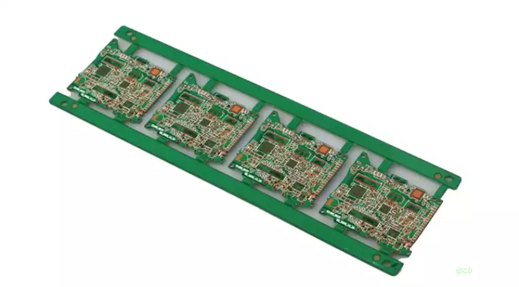
A bluetooth player circuit board has to do more than receive music wirelessly. It must transfer audio data from a connected device, process the stream, convert it into a usable audio signal, and deliver that signal to headphones, an external amplifier, or speakers. Each stage has different electrical requirements, and the way they are connected on the PCB can affect sound quality, wireless stability, power consumption, and the overall size of the finished product.
The challenge becomes more noticeable when several functions share a compact bluetooth player circuit board. The Bluetooth radio operates at 2.4 GHz, the audio section may handle low-level analog signals, and the power amplifier can carry rapidly changing currents. A successful design needs to accommodate all three without allowing radio activity or power switching to introduce unwanted noise into the audio path.
The Audio Signal Does Not End at the Bluetooth Receiver
When a phone or computer streams music to a player, the Bluetooth section receives the wireless data and passes it to the audio-processing circuitry. Depending on the architecture, decoding and digital audio processing may be handled by a Bluetooth audio SoC, a separate processor, or a dedicated audio codec. The signal may then pass through a digital-to-analog converter before reaching an analog output stage.
Not every bluetooth player circuit board uses the same architecture. A compact audio receiver may integrate wireless connectivity and audio processing into one device, while a more flexible player may use separate components for wireless communication, storage, display control, audio conversion, and amplification. The appropriate arrangement depends on the required audio formats, output type, user interface, and power budget.
These choices affect the PCB from the beginning. Digital audio interfaces such as I²S require suitable routing between the processor and codec, while analog signals need a layout that limits unwanted noise and interference. If the board includes a headphone output, its amplifier and output connector must be placed with the audio path and mechanical enclosure in mind.
The design should also distinguish between line-level audio and speaker-level output. A line output is intended to feed another audio stage, whereas a speaker output must deliver enough current to drive the connected load. Mixing these requirements during circuit planning can lead to an unsuitable amplifier, unnecessary power consumption, or an output stage that does not match the intended product.
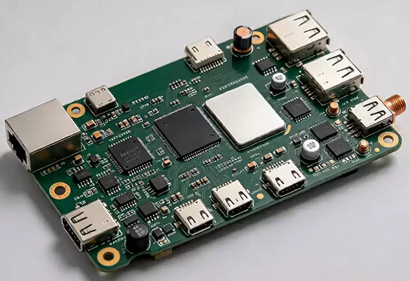
When Wireless Performance and Sound Quality Compete for Space
A Bluetooth antenna needs an appropriate RF environment to operate as intended. Its position, clearance, ground structure, and proximity to conductive objects can affect wireless performance. On a compact player board, however, the same area may be needed for a display, buttons, connectors, battery circuitry, or the audio amplifier.
Placing the antenna close to a metal enclosure, display structure, or other conductive part can change its behavior. The final mechanical assembly therefore matters just as much as the bare PCB layout. Antenna placement should be planned early, with the module or antenna manufacturer’s layout and keepout recommendations followed wherever applicable.
The audio section presents a different concern. Low-level analog signals can pick up interference from switching power supplies, digital clocks, and amplifier output currents. A board may pass basic connectivity checks while still producing audible hiss, buzzing, or tones that vary with processor activity or wireless operation.
Component placement can help control these interactions. The RF section, audio conversion circuitry, sensitive analog paths, power conversion, and speaker amplifier should be arranged according to their functions and noise characteristics. A continuous ground reference is often preferable to arbitrary ground-plane splits, provided that return currents and noisy power paths are managed appropriately.
The speaker amplifier deserves particular attention when it uses a switching architecture such as Class D. Its output carries high-frequency switching components in addition to the audio signal. Keeping the relevant current loops compact and avoiding unnecessary proximity to the antenna and sensitive analog inputs can help reduce unwanted coupling.
Power Design Determines More Than Battery Life
Portable Bluetooth players often need to power the wireless section, processor, display, audio codec, amplifier, and battery-management circuitry from the same source. These loads behave differently. The radio and processor can change their current demand during operation, while a speaker amplifier may draw substantial current when the audio level increases.
The power architecture needs to accommodate these variations without allowing supply disturbances to affect sensitive circuitry. Local decoupling, suitable regulator selection, and careful routing of high-current paths are important parts of the design. Where separate supply filtering is needed for analog and digital sections, it should be planned around the actual current paths rather than added without considering the full circuit.
Battery charging also affects bluetooth player circuit board layout. A charging circuit may need to handle thermal dissipation and provide suitable protection, while the battery connector and power path must be designed for the expected current. If the product supports USB charging and audio playback at the same time, the designer should evaluate whether switching noise from the charging circuit can reach the audio output.
Heat becomes more important as the player integrates more functions. The amplifier, charging circuit, and voltage regulators may all dissipate power in a limited area. Component spacing, copper areas, thermal vias where appropriate, and the enclosure’s ability to release heat can influence the board’s operating temperature.
A well-planned bluetooth player circuit board balances these requirements rather than optimizing each power rail in isolation. The goal is to maintain stable operation during pairing, playback, charging, and changes in audio output level.
What to Check Before the Bluetooth Player Circuit Board Goes Into Production
A prototype should be evaluated as a complete audio product, not just as a populated PCB. Wireless pairing and connection stability need to be checked in the intended enclosure, because antenna performance can change after the board is installed. Audio testing should cover the expected output load and operating levels, with attention to background noise, distortion, channel balance, and unexpected sounds during wireless activity.
Power testing should include charging, startup, standby, and playback under realistic conditions. If the player contains a display, buttons, storage, or other peripherals, those functions should be tested while audio is playing. This helps reveal interference that may not appear when each section is tested separately.
Manufacturing documentation also needs to match the final design revision. The schematic, PCB layout, bill of materials, assembly drawings, and firmware assumptions should remain consistent. Connectors, switches, displays, and antenna clearances need to be checked against the enclosure before the design is released for a larger run.
A bluetooth player circuit board works well when wireless reception, audio processing, amplification, and power management are treated as one connected system. The most important decisions are often the relationships between these sections: where the antenna sits, how the audio signal is routed, how amplifier current returns to ground, and how power noise is kept away from sensitive circuitry. Getting these relationships right gives the finished player a better foundation for reliable wireless playback and clean audio output.