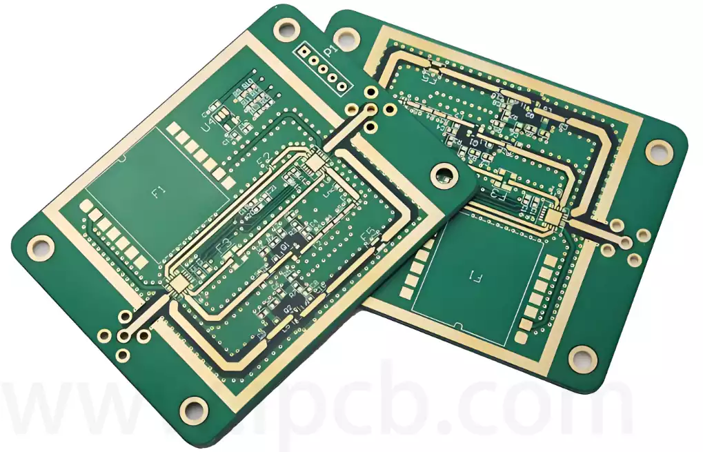
As electronic equipment continues to demand higher power density and greater operational stability, ceramic circuit boards have seen increasing adoption in high-end manufacturing sectors due to their excellent thermal conductivity, high dielectric strength, and superior resistance to high temperatures. Compared with conventional FR-4 PCBs, ceramic circuit boards are generally much more expensive. This price gap is not the result of a single factor, but rather the combined outcome of material characteristics, manufacturing processes, and market-scale constraints.
Substrates and Auxiliary Materials
Conventional PCBs primarily use FR-4 epoxy glass fiber laminate as the base material. This material system is technologically mature, widely available, and benefits from large-scale production, resulting in relatively low unit costs. In contrast, ceramic circuit boards must simultaneously meet stringent requirements for high thermal conductivity, low thermal expansion, and strong electrical insulation. As a result, mainstream substrate choices are limited to ceramic materials such as alumina, aluminum nitride, and zirconia. The intrinsic properties of these materials, along with their demanding production requirements, establish a much higher cost baseline than that of standard PCB substrates.
Among them, alumina ceramic is the most widely used substrate material for ceramic circuit boards. Alumina ceramics intended for electronic applications must maintain a high level of purity, typically above 95%, with some high-performance applications requiring purities as high as 99.6%. Producing high-purity alumina involves multiple stages, including raw material selection, high-temperature calcination, and fine grinding. Each step requires strict control of impurity levels, as even trace contaminants can adversely affect the final product’s thermal conductivity and insulation performance.
Aluminum nitride ceramics offer significantly higher thermal conductivity than alumina, but their manufacturing process is even more complex. They are produced by reacting high-purity aluminum powder with nitrogen at temperatures exceeding 1800°C, under strictly controlled oxygen-free conditions to prevent oxidation that would degrade performance. These stringent processing requirements make aluminum nitride substrates substantially more expensive than alumina, directly increasing the material cost of the corresponding ceramic circuit boards.
Significant differences also exist between ceramic circuit boards and conventional PCBs in terms of conductor and auxiliary material selection. Standard PCBs typically use conventional copper foil, which is easy to process and relatively low in cost. Ceramic circuit boards, however, must withstand high-temperature and high-frequency operating environments, so their conductors often use oxygen-free copper with a purity of 99.9% or higher. In certain specialized applications, gold or silver may even be used for circuitry or interconnections. Oxygen-free copper offers superior electrical conductivity and oxidation resistance, but it is more expensive to procure and more complex to process than standard copper foil. Precious metals such as gold and silver provide excellent performance but come with inherently high raw material costs, even when used in small quantities.
Moreover, ceramic substrates and metal conductors exhibit inherent differences in thermal expansion coefficients. To ensure stable bonding between the two, intermediate layers made of materials such as titanium or tungsten are often introduced. The cost of these auxiliary materials must also be factored into the total manufacturing cost of ceramic circuit boards.
Manufacturing Processes
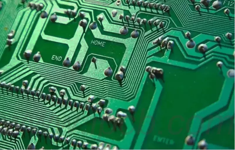
The production of conventional PCBs has reached a high level of automation. Processes such as panel cutting, drilling, etching, solder mask application, and silkscreen printing are highly standardized and efficient. A single production line can process tens of thousands of boards per day, allowing manufacturing costs to be significantly diluted on a per-unit basis.
Ceramic circuit board manufacturing, by contrast, faces far greater technical challenges. The process flow is more complex, parameter control requirements are stricter, and overall automation levels are lower. In addition, yield rates are generally lower than those of standard PCBs. These factors combine to substantially increase the manufacturing cost per unit.
Metallization is a core process in ceramic circuit board production, as it enables strong bonding between metal conductors and ceramic substrates. Common metallization methods include thick-film printing, thin-film deposition, and Active Metal Brazing (AMB), each with its own technical challenges.
In thick-film printing, metal paste is applied to the ceramic substrate via screen printing and then sintered at high temperatures ranging from 850°C to 950°C. During sintering, temperature uniformity and heating and cooling rates directly affect conductor adhesion and electrical performance. Excessively high temperatures can cause substrate deformation or cracking, while insufficient temperatures result in incomplete sintering and poor conductor stability. As a result, manufacturers must invest in high-precision tunnel furnaces, which are costly to purchase and energy-intensive to operate. Additionally, the screen masks used in thick-film printing must maintain micron-level aperture accuracy, making their fabrication and maintenance more expensive than the etching masks used in conventional PCB processes.
Thin-film deposition processes, such as sputtering and evaporation, can achieve ultra-fine line widths below 10 μm and are well suited for high-frequency, high-density ceramic circuit boards. However, these processes must be carried out in high-vacuum environments, requiring significant capital investment in vacuum deposition equipment. Production cycles are also much longer—thin-film deposition on a single ceramic circuit board may take several hours, whereas conventional PCB etching typically takes only tens of minutes. Furthermore, thin-film conductors are relatively thin and exhibit lower wear resistance and peel strength, necessitating additional steps such as electroplating thickening and passivation, which further increase process complexity and production time.
Active Metal Brazing (AMB) is widely used for high-power ceramic circuit boards. This process introduces brazing alloys containing active elements such as titanium or zirconium between the ceramic substrate and metal layers, forming a strong metallurgical bond at elevated temperatures. While AMB offers excellent bonding strength and thermal performance, it imposes extremely strict requirements on production conditions and process control. Brazing must be performed under high vacuum or inert gas protection to prevent oxidation, and the temperature must be precisely controlled near the melting point of the filler metal (typically 800–1000°C). Temperature deviations exceeding ±5°C can lead to bonding failure. Cooling must also be carefully controlled to mitigate thermal stress between the ceramic and metal layers and prevent cracking. Due to these stringent requirements, AMB yield rates often range between 70% and 80%, significantly lower than the 95% or higher yields common in conventional PCB manufacturing. The material and processing costs of rejected parts are ultimately absorbed by the qualified products, further increasing unit costs.
Market and Supply Chain Factors
The conventional PCB industry is highly mature, with large market demand and well-established supply chains. Economies of scale are significant, allowing raw material procurement, equipment depreciation, and labor costs to be effectively diluted through high-volume production. Ceramic circuit boards, however, remain a niche segment, with applications primarily in aerospace, new energy vehicles, and high-end medical equipment. Market demand is relatively limited, making it difficult to achieve similar scale efficiencies and resulting in a range of hidden costs.
From a technology development perspective, ceramic circuit boards evolve rapidly, and performance requirements vary widely across application scenarios. For example, aerospace applications may require radiation resistance and lightweight structures, while ceramic circuit boards used in electric vehicle charging systems prioritize high-temperature and high-voltage endurance. To meet these diverse and customized requirements, manufacturers must continually invest in specialized R&D efforts, including ceramic material optimization, process parameter refinement, and dedicated equipment modification. Due to limited market volumes, these R&D investments cannot be spread across large production runs and therefore must be allocated to individual products.
Quality inspection requirements for ceramic circuit boards are also more stringent. In addition to standard dimensional and electrical tests, advanced inspection methods such as X-ray analysis, ultrasonic testing, and thermal resistance measurements are often required to evaluate internal bonding quality, thermal performance, and insulation characteristics. The acquisition and maintenance of such specialized testing equipment add further operational costs.
Supply chain constraints represent another source of hidden cost. Core raw materials for ceramic circuit boards—such as high-purity ceramic powders, oxygen-free copper, and specialized brazing alloys—are supplied by a relatively small number of vendors, limiting competition and reducing pricing flexibility. Manufacturers have limited bargaining power, and procurement costs tend to remain rigid. Additionally, ceramic circuit boards are typically produced in small batches, and some customers impose tight delivery schedules. Suppliers may therefore increase minimum order quantities or charge expedited fees, further raising procurement costs.
Logistics and storage costs are also higher. Ceramic substrates are inherently brittle and require specialized shock-resistant and moisture-controlled packaging during transportation. Storage environments must remain dry and temperature-stable, making logistics and warehousing more expensive than for standard PCB materials.
Labor costs represent another important factor. Ceramic circuit board manufacturing places higher demands on operator expertise. While conventional PCB production lines are highly automated and operators can be trained quickly, critical ceramic circuit board processes—such as paste formulation for thick-film printing or parameter control in AMB processes—often require skilled technicians with extensive experience. These technicians require longer training periods and command higher wages, and their labor costs are ultimately reflected in product pricing.
The high cost of ceramic circuit boards is the result of multiple objective factors, including demanding material performance requirements, complex manufacturing processes, and limitations imposed by market scale. It is not the outcome of arbitrary price inflation. As emerging industries such as new energy, 5G, and artificial intelligence continue to grow, demand for high-power, high-reliability electronic components is steadily increasing, and the market for ceramic circuit boards is gradually expanding. For end users, the primary motivation for choosing ceramic circuit boards lies in their ability to operate reliably under conditions that conventional PCBs cannot withstand. Their high-temperature resistance, superior thermal conductivity, and low-loss characteristics help improve system stability and reduce failure rates, delivering tangible value over the long term.