HDI multilayer PCB represent a significant advancement in printed circuit board technology. They are essential components in many modern electronic devices, offering numerous advantages over traditional PCBs. This article delves into the intricacies of HDI multilayer PCBs, exploring their structure, benefits, applications, and the manufacturing processes involved.
The Structure of HDI Multilayer PCBs
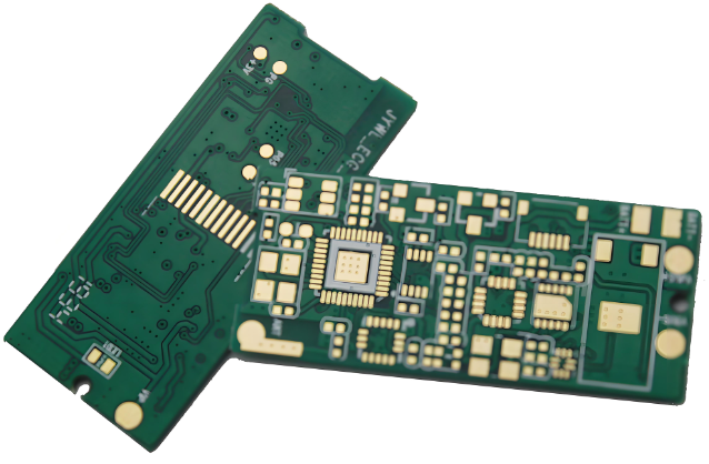
HDI multilayer PCBs are distinguished by their compact design, which allows for a higher density of components. They achieve this through the use of microvias, blind vias, and buried vias. These vias are much smaller than those used in conventional PCBs, enabling more interconnections in a smaller area.
Microvias are tiny holes that connect adjacent layers within the PCB. They are typically laser-drilled, ensuring precision and reliability. Blind vias connect an outer layer to one or more inner layers but do not pass through the entire board. Buried vias, on the other hand, connect internal layers without reaching the surface. This combination of vias allows for a more complex and dense layout, accommodating more components and functionality.
Benefits of HDI Multilayer PCBs
The primary advantage of HDI multilayer PCBs is their ability to support higher component density. This is crucial in modern electronics, where devices are continually becoming smaller and more powerful. HDI technology enables the integration of more functionality into a compact space, which is essential for applications like smartphones, tablets, and wearable devices.
Another significant benefit is improved electrical performance. The shorter interconnect paths reduce signal loss and delay, enhancing the overall performance of the device. Additionally, HDI multilayer PCBs offer better thermal management. The higher density of vias provides more paths for heat dissipation, which is critical in high-power applications.
HDI multilayer PCBs also offer greater design flexibility. Designers can create more complex circuits without the constraints of traditional PCB design limitations. This flexibility enables the development of innovative and sophisticated electronic devices.
Applications of HDI Multilayer PCBs
HDI multilayer PCBs are ubiquitous in modern electronics. They are a key component in consumer electronics such as smartphones, tablets, laptops, and wearable devices. The compact size and high performance of HDI PCBs make them ideal for these applications.
In the automotive industry, HDI multilayer PCBs are used in advanced driver-assistance systems (ADAS), infotainment systems, and engine control units (ECUs). The high reliability and performance of HDI PCBs are crucial in these safety-critical applications.
HDI multilayer PCBs are also prevalent in the aerospace and defense sectors. They are used in avionics, radar systems, and other critical applications where reliability and performance are paramount. The ability to pack more functionality into a smaller space is particularly valuable in aerospace applications, where weight and space are at a premium.
In the medical field, HDI multilayer PCBs are used in diagnostic equipment, patient monitoring systems, and implantable devices. The high reliability and compact size of HDI PCBs make them suitable for these life-saving applications.
Manufacturing Processes for HDI Multilayer PCBs
The manufacturing of HDI multilayer PCBs involves several advanced processes. The first step is the creation of the core layers, which are typically made of fiberglass-reinforced epoxy laminate sheets. These core layers are then laminated together under high pressure and temperature to form a solid base.
Next, the vias are drilled. This step involves both mechanical and laser drilling. Mechanical drilling is used for larger vias, while laser drilling is employed for microvias. The precision of laser drilling is crucial for creating the tiny vias required in HDI multilayer PCBs.
After drilling, the vias are plated with copper to create electrical connections between the layers. This process, known as electroplating, ensures that the vias are conductive and reliable. The PCB is then etched to create the desired circuit patterns. This involves coating the board with a photoresist, exposing it to UV light through a mask, and then developing the exposed photoresist to reveal the copper underneath. The exposed copper is then etched away, leaving behind the desired circuit pattern.
Finally, the PCB is coated with a solder mask to protect the circuitry and to prevent solder bridges during component assembly. The solder mask also improves the durability and reliability of the PCB. Surface finish options such as HASL (Hot Air Solder Leveling), ENIG (Electroless Nickel Immersion Gold), and OSP (Organic Solderability Preservatives) are applied to the exposed copper pads to ensure good solderability and long shelf life.
Challenges in HDI Multilayer PCB Manufacturing
Despite the numerous advantages of HDI multilayer PCBs, their manufacturing presents several challenges. The precision required for drilling microvias and the complexity of multilayer lamination make the manufacturing process more demanding and costly compared to traditional PCBs.
The high density of components and interconnections also increases the risk of manufacturing defects. Ensuring the reliability of such densely packed boards requires rigorous testing and quality control. Advanced inspection techniques such as Automated Optical Inspection (AOI) and X-ray inspection are often employed to detect defects that are not visible to the naked eye.
Thermal management is another challenge in HDI multilayer PCB manufacturing. The high density of components generates more heat, which must be effectively dissipated to prevent overheating and ensure the reliability of the device. This requires careful design and the use of materials with good thermal conductivity.
Future Trends in HDI Multilayer PCB Technology
The demand for HDI multilayer PCBs is expected to continue growing as electronic devices become more compact and powerful. Several trends are likely to shape the future of HDI technology.
One significant trend is the increasing use of advanced materials. High-performance laminates with better thermal and electrical properties are being developed to meet the demands of next-generation electronic devices. These materials will enable even higher component densities and improved performance.
Another trend is the integration of more advanced manufacturing processes. Techniques such as 3D printing and additive manufacturing are being explored for PCB production. These processes offer the potential for greater design flexibility and reduced manufacturing costs.
The development of more advanced inspection and testing techniques is also expected to play a crucial role in the future of HDI technology. As HDI multilayer PCBs become more complex, ensuring their reliability will require more sophisticated inspection methods.
Environmental Considerations in HDI PCB Manufacturing
As the electronics industry grows, so does its environmental impact. HDI multilayer PCB manufacturing involves various chemicals and processes that can be harmful to the environment. Therefore, it is essential for manufacturers to adopt sustainable practices.
One approach is to use environmentally friendly materials. Lead-free solders and halogen-free laminates are examples of materials that reduce the environmental impact of PCBs. Additionally, recycling and proper disposal of waste materials can minimize the ecological footprint of PCB manufacturing.
Energy efficiency is another critical aspect. Manufacturing processes that consume less energy and reduce carbon emissions are increasingly important. Implementing energy-efficient technologies and optimizing manufacturing processes can contribute to a more sustainable industry.
Water usage is also a concern in PCB manufacturing. The processes involved often require significant amounts of water, which can be reduced through recycling and purification systems. By implementing water-saving technologies, manufacturers can lessen their environmental impact.
Regulatory Compliance and Quality Standards
HDI multilayer PCB manufacturers must adhere to various regulatory requirements and quality standards to ensure product reliability and safety. Compliance with standards such as ISO 9001 (Quality Management Systems), ISO 14001 (Environmental Management Systems), and IPC standards (Association Connecting Electronics Industries) is crucial.
ISO 9001 ensures that manufacturers maintain consistent quality in their products. This standard requires a robust quality management system, regular audits, and continuous improvement practices.
ISO 14001 focuses on environmental management. Manufacturers certified under this standard must demonstrate their commitment to minimizing environmental impact through sustainable practices and continuous monitoring.
IPC standards provide specific guidelines for PCB manufacturing, including design, materials, and testing procedures. Compliance with IPC standards ensures that PCBs meet industry benchmarks for performance and reliability.
Advancements in HDI PCB Design Tools
The design of HDI multilayer PCBs requires sophisticated software tools. Recent advancements in design tools have significantly improved the efficiency and accuracy of PCB design.
Computer-Aided Design (CAD) software has become more powerful, offering features such as automatic routing, real-time simulation, and integrated component libraries. These tools allow designers to create complex PCB layouts with greater ease and precision.
Simulation tools have also advanced, enabling designers to test their PCB designs virtually before manufacturing. These simulations can identify potential issues such as signal integrity problems, thermal management challenges, and mechanical stresses. By addressing these issues early in the design process, manufacturers can reduce the risk of defects and improve the overall quality of the final product.
Cloud-based design platforms are another innovation in PCB design. These platforms facilitate collaboration among design teams, allowing multiple designers to work on the same project simultaneously. This collaborative approach can speed up the design process and ensure that all aspects of the PCB are thoroughly reviewed and optimized.
Integration of HDI PCBs with Other Technologies
The integration of HDI multilayer PCBs with other emerging technologies is opening up new possibilities in electronics design. One notable example is the combination of HDI PCBs with flexible and rigid-flex PCBs.
Flexible PCBs are made from flexible materials, allowing them to bend and conform to various shapes. Rigid-flex PCBs combine rigid and flexible layers, providing both durability and flexibility. Integrating HDI technology with flexible and rigid-flex PCBs enables the creation of highly versatile and compact electronic devices.
Another area of integration is with advanced semiconductor packaging techniques such as System-in-Package (SiP) and Chip-on-Board (CoB). These techniques involve placing multiple semiconductor chips and components onto a single substrate, often an HDI PCB. This integration allows for higher performance and greater functionality in a smaller footprint.
The Internet of Things (IoT) is also driving the integration of HDI PCBs with sensors, wireless communication modules, and other IoT components.