Transparent flexible PCBs, possessing both flexibility and light transmission properties, hold immense application potential across multiple fields. Their design necessitates balancing material performance with routing strategies. This article systematically outlines core design considerations from two perspectives: material selection and routing optimisation.
Common Materials for Transparent Flexible PCBs
Substrates
Polyimide (PI): High-temperature resistance (400°C transient), high tear strength (15,000–30,000 PSI), suitable for high-end applications such as aerospace and medical devices. However, it exhibits low light transmittance (approximately 85%) and carries a higher cost.
Polyester (PET): Transmittance exceeding 92%, low cost, excellent flexibility (glass transition temperature Tg=80°C), suitable for consumer electronics. However, it exhibits poor temperature resistance (melting point 250°C) and is only applicable to low-temperature soldering processes.
Transparent Polycarbonate (PC): Offers light transmittance comparable to PET with superior impact resistance, but exhibits higher moisture absorption (0.4%), necessitating surface coating optimisation.
Conductive Layer
Metal Mesh: Light transmittance above 90%, sheet resistance as low as 0.1Ω/sq, suitable for high-precision touch modules. However, line width must be <5μm to prevent moiré patterns, and the process complexity is high.
Nano-silver wires (AgNWs): Light transmittance comparable to ITO, excellent flexibility (bending radius <1mm), suitable for dynamic bending applications. However, prolonged bending may cause silver migration, necessitating protection via a polyurethane encapsulation layer.
Transparent Conductive Oxides (TCO): ITO offers over 95% light transmittance with sheet resistance as low as 10Ω/sq, suitable for static displays. However, its high brittleness necessitates patterning via laser etching or photolithography processes.
Covering Film and Bonding Layer
Covering Film: Utilises flexible materials compatible with the substrate (e.g., polyimide or polyester), with a thickness of 10–50μm, providing insulation and mechanical protection.
Bonding Layer: Acrylic or epoxy resin materials, 0.01–0.05mm thick, requiring low flow properties and thermal expansion coefficient (CTE) matching.
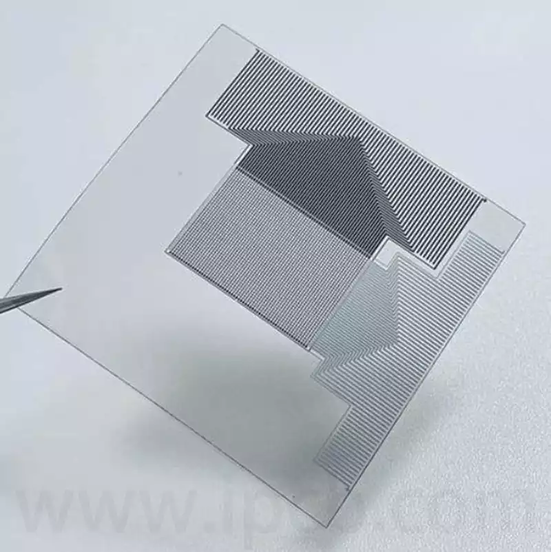
Routing Strategy for Transparent Flexible PCBs
Trace Width Design
Dynamic Bending Scenarios: Trace width must be determined based on the bending radius (R) and copper foil thickness (t), adhering to the empirical formula w ≤ R/20 (unit: μm) to prevent copper foil fracture due to stress concentration during bending. For instance, with a bending radius of 1mm, a trace width ≤50μm is recommended.
Current Carrying Capacity: Calculate trace width per IPC-2221 standards to ensure target current is carried within permissible temperature rise limits. For instance, 1A current requires ≥100μm trace width on 1oz copper foil (35μm thickness).
Spacing Control
Safety Spacing: Adjacent trace spacing must meet electrical insulation requirements, typically ≥2 times the line width and no less than 50μm (further increase required for high-frequency signals).
Bend Compensation: Increase trace spacing in bend areas (recommended 20%-30% increase) to prevent short circuits caused by friction or compression during bending.
Corner Design and Trace Orientation for Transparent Flexible PCBs
Curved Corner Design
Avoid 90° right-angle corners; employ curved transitions (radius ≥ 3× trace width) to distribute bending stresses. For example, with a 50μm trace width, a minimum radius of ≥150μm is recommended.
For high-frequency signal traces, curved corners also reduce signal reflection, improving signal integrity.
Trace Orientation Along Bending Axis
Align traces as parallel as possible to the bending axis to minimise tensile stress perpendicular to the bend direction. For instance, in foldable screen hinge regions, signal traces should run along the hinge axis.
Where crossing traces are unavoidable, employ diagonal intersections (45° angles) or interlayer crossings (via vias) to prevent stress accumulation from perpendicular intersections.
Via and Pad Design for Transparent Flexible PCBs
Via Placement
Positioning: Vias should be positioned away from bending zones (minimum distance ≥2mm) to prevent wall fracture under bending stress.
Quantity Optimisation: Minimise via count to reduce discontinuity risks in signal paths; where multiple vias are essential, employ staggered arrangements to distribute stress.
Dimensioning: Via diameter ≥0.2mm and pad diameter ≥0.4mm are recommended to ensure soldering reliability. For high-frequency signals, vias must meet impedance matching requirements.
Pad Reinforcement
Apply coverlay or PI reinforcement sheets beneath pads to enhance adhesion strength between pads and substrate, preventing pad delamination during bending.
For large pads (e.g., BGA pads), employ cross-shaped or grid-shaped window designs to reduce stress differentials between pads and substrate.
Signal Layering and Shielding for Transparent Flexible PCBs
Layering Strategy
High-frequency signal layers: Dedicated placement for high-frequency signals (e.g., MIPI, USB 3.0) to avoid interference with other signals; employ stripline or microstrip structures to control characteristic impedance (e.g., 50Ω).
Power/ground layers: Allocate separate layers for power and ground to reduce power noise; enhance thermal dissipation through large-area copper ground planes.
Low-Speed Signal Layer: Centralise low-speed signals (e.g., buttons, LEDs) to simplify routing complexity.
Shielding Design
Form shielding layers by grounding both sides of sensitive signals (e.g., antenna signals). For high-frequency signals, employ metal mesh or nano-silver shielding films with ≥90% light transmittance.
Reduce interlayer crosstalk by increasing insulation thickness (e.g., ≥50μm) or inserting conductive adhesive between layers.
Dynamic Bend Zone Treatment
Serpentine Routing
Employ serpentine routing in bend zones to absorb strain during flexing by increasing trace length, thereby reducing stress per unit length. For instance, with a bending radius of 0.5mm, the serpentine routing period should be ≤1mm and amplitude ≤0.3mm.
Serpentine routing must maintain symmetry to prevent localised stress concentration from asymmetry.
Stress Relief Structures
Incorporate dumbbell-shaped or elliptical cutouts on both sides of the bending zone to release substrate stress; Window width should be ≥0.5mm, with length adjusted according to bend zone dimensions.
Fill windowed areas with a flexible adhesive layer (e.g., silicone) to enhance mechanical buffering.
Transparent flexible PCB design requires precise alignment of material properties with routing strategies. Through judicious material selection and meticulous routing, performance and reliability in complex scenarios can be significantly enhanced, providing critical support for the innovative development of flexible electronic devices.
