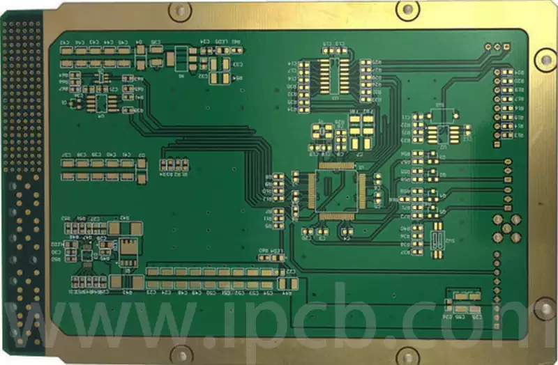
What is a presensitized PCB board?A presensitized pcb board is a special type of printed circuit board with a photosensitive surface. It supports photolithography technology and can be adjusted using ultraviolet light. Despite common misconceptions, presensitized PCBs are similar to standard copper-clad PCBs, but essentially involve transferring graphics onto the board. Presensitized printed circuit boards incorporate unique photosensitivity during manufacturing. They transfer special image coatings onto the board through exposure to ultraviolet light.
What materials are used in presensitized PCB board?
Teflon
Polytetrafluoroethylene is a versatile, durable, and compact material used in presensitized PCB board. It has high elasticity because it does not expand rapidly in hot weather.
Metals
Most PCB development typically requires three metals: copper, iron, and aluminium. Copper is the most well-known, which is why most PCBs are copper-plated.
Prepreg
Prepreg is a resin-impregnated thermoplastic. The resin is pre-dried, but its purpose is not to flow, follow, and fully reduce when heated.
FR-4 Epoxy Resin
FR-4 is one of the most commonly used epoxy resins. FR-4 glass epoxy resin is a well-known thermoplastic coating with excellent toughness. It consists of glass-reinforced fabric with epoxy resin fasteners, offering electrical, mechanical, and thermal efficiency.
Polyimide
Polyimide laminates are more heat-resistant than FR4 epoxy resin and also have better electrical durability to some extent. Additionally, they are more expensive than FR4.
Presensitized PCB boards are similar to conventional copper-clad PCBs, with the main difference being how the design is transferred to the board.
Conventional (copper-clad) PCBs transfer images using the following methods:
- Toner transfer method
- Inkjet mask method
- Dry film photopolymer method
The innovative liquid film method is used.
Presensitized PCB boards transfer images using the following methods:
- Exposure to ultraviolet light
During manufacturing, a special photosensitive coating is added to the presensitized PCB board. The photosensitive coating is highly sensitive to light! A ‘release’ layer protects the unique photosensitive coating from accidental exposure. The peelable protective layer must be removed immediately before exposure to ultraviolet light!
How to make a presensitized PCB board
Provide inner layer material:
Provide an inner layer made of thermosensitive resistor material. This inner layer should include a thermosensitive resistor base layer, two copper layers on either side of the thermosensitive resistor base layer, and two thin nickel protective layers on the side of the copper layers facing away from the thermosensitive resistor base layer. The thin nickel protective layer serves to protect the copper layers and prevent damage to the inner layer board during processing. The thickness of the inner layer board material can be set to 0.27 mm. Prior to processing, the inner layer board must undergo testing using a ternary device to ensure compliance with specifications.
Inner layer processing
Nickel Removal Treatment: The inner layer board is immersed in a mixed acid solution for nickel removal treatment to remove the thin nickel protective layer from the surface of the inner layer board. The mixed acid typically consists of nitric acid and citric acid, with a concentration of 30%, temperature controlled at 25-35°C, and a treatment time of 90 seconds. This ensures stable removal of the thin nickel protective layer while avoiding damage to the copper layers.
Etching, Drilling, Inner Layer Circuitry, Inner Layer Etching: Successively perform etching, drilling, inner layer circuitry, and inner layer etching on the copper layer of the inner layer board.
Etching: Remove unnecessary copper from the circuit board through corrosion, leaving the required portions:
Drilling: Use a drill bit to process holes on the inner layer board.
Inner layer routing: Create an inner layer routing protective layer on the inner layer board.
Inner layer etching: Corrode the copper surface of the inner layer board while retaining the copper surface covered by the inner layer routing protective layer, forming the inner layer routing.
Optical inspection and brownisation treatment: During the entire inner layer processing, each inner layer board must undergo inspection using automatic optical inspection equipment. After optical inspection, brownisation treatment can be performed to remove oils and impurities from the surface of the inner layer board, increase surface cleanliness, and enhance the bonding strength between the inner layer board and polypropylene.
Lamination and Outer Layer Preparation
Lamination: Multiple inner layers are bonded together at a predetermined lamination temperature and pressure to form a single unit as the outer layer. Polypropylene (PP) adhesive can be used for bonding, with a PP layer thickness of approximately 0.08 mm. The lamination temperature threshold should be less than or equal to 170°C to ensure resin curing and surface adhesion, thereby enhancing the reliability of inner layer interconnections.
Outer Layer Board Drilling and Cleaning Activation: Drill holes in the outer layer board. After drilling, place the outer layer board in a plasma cleaner for de-adhesion and activation treatment. The plasma cleaner uses a mixture of oxygen, nitrogen, and carbon tetrafluoride gas ionised under high voltage to form plasma gas, which is then used to bombard the walls of the holes in the outer layer board. The mixing ratio of oxygen, nitrogen, and carbon tetrafluoride in the mixed gas is 2:5:2. The bombardment of the hole walls lasts for 60 minutes. This process cleans and modifies the hole walls, performs photoresist ash removal, roughens the surface of the hole walls, and forms micro-pits, thereby improving the adhesion and wetting performance of subsequent chemical copper plating.
Outer Layer Circuitry and Protection
Chemical Copper Plating and Pulse Electroplating: Chemical copper plating and pulse electroplating are performed sequentially. Chemical copper plating deposits a layer of copper between the copper layers within the holes of the outer layer board. Pulse electroplating deposits a copper layer of a pre-set thickness threshold on the surface and walls of the outer layer board, with the electroplated hole copper thickness being greater than or equal to 28 μm and the surface copper thickness being 61 ± 10 μm.
Outer Layer Circuitry and Acid Etching: A protective layer for the outer layer circuitry is formed on the outer layer board. Acid etching is then performed to corrode the copper surface of the outer layer board while preserving the copper surface covered by the protective layer, thereby forming the outer layer circuitry. The outer layer board after electroplating must be inspected using an automatic optical inspection device.
Solder Mask and Nickel-Tin Plating: A protective film is applied to the surface of the outer layer board after optical inspection. After the protective film is applied, the outer side of the outer layer board is subjected to nickel-tin plating. The nickel thickness is 4.6±2.5 μm, and the tin thickness is 12.7±5 μm. The nickel-tin plating process enhances high-temperature resistance, salt spray resistance, reduces internal stress in the plating layer, prevents bubbling and peeling, and extends the service life of the PCB.
Final inspection: After solder resist application, the outer layer board undergoes final inspection to ensure product quality.
Applications of presensitized PCB board:
Consumer devices
PCBs are essential for the operation of mobile phones, laptops, and various other consumer devices. As we integrate electronics into more products, PCBs are becoming an integral part of daily life.
Automotive components
Electrical equipment is becoming increasingly common in vehicles. In such cases, PCBs are employed.
Aircraft components
Avionics and presensitized pcb board shares similar decisions with the automotive industry,
Marine applications
Various vessels and frameworks rely on PCBs to function. This includes small boats, large cargo ships, submarines, communication systems, and transportation equipment.
Health and safety equipment
Many components of safety frameworks, whether in homes, organisations, or government institutions, rely on presensitized pcb board.
Media communication equipment
PCBs are a foundational component of the media communication industry. They are crucial for consumer devices such as mobile phones and walkie-talkies, as well as for the frameworks that support their operation.
Presensitized PCB board technology simplifies the image transfer process, facilitating the manufacture of custom PCBs and playing a key role in the development and production of various electronic products. As electronic technology continues to advance, PCBs and their manufacturing processes will also evolve to meet the demands of higher performance and more complex designs.