Engineering Significance and Application Background of Impedance Control PCBs
In high-speed electronic systems, signal transmission is no longer simply a matter of “connection is sufficient.” As signal frequencies increase and rise times become steeper, PCB traces themselves have evolved from simple conductors into transmission structures with defined electrical characteristics. It is against this backdrop that impedance control PCBs have become an indispensable part of high-speed electronic design. It is not a synonym for a specific process, but rather a systematic engineering requirement that permeates the entire design, materials, and manufacturing process.
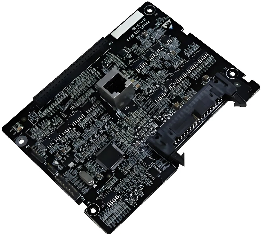
Essentially, the core objective of impedance control is to ensure that signals remain stable and predictable during transmission. When a signal propagates along PCB traces, a sudden change in line impedance can cause phenomena such as reflection, overshoot, or ringing. These problems may not be noticeable in low-speed systems, but in high-speed or high-frequency applications, they directly affect signal integrity, leading to increased bit error rates, timing failures, and even system malfunctions. Therefore, impedance control PCBs are not about “raising the performance ceiling,” but about ensuring that the system operates stably within its design performance range.
In modern electronic products, the need for impedance control has gradually expanded from communication equipment to many other fields. High-speed interfaces, precision control systems, and applications sensitive to signal stability are increasingly reliant on impedance-controlled PCB structures. In this context, the PCB is no longer merely a platform for components, but an integral part of the signal chain. Designers need to precisely plan the width, spacing, layer stack-up, and reference planes of PCB traces, treating them like the circuit itself.
It’s important to note that impedance control PCBs cannot be achieved solely through design calculations. The theoretical impedance value must be realized through material properties and manufacturing processes. The dielectric constant of the dielectric material, copper foil thickness, lamination tolerances, and etching precision all directly impact the final impedance. Therefore, impedance control is not solely the responsibility of the design department, but a collaborative effort involving design, material selection, and PCB manufacturing capabilities.
From a manufacturing perspective, the introduction of controllable impedance implies higher consistency requirements. While standard PCBs allow for a certain range of dimensional and material variations, impedance control PCBs require these variables to be controlled within stricter limits. This not only increases manufacturing complexity but also imposes higher standards on process control and quality verification, such as the introduction of impedance testing and process compensation mechanisms.
In general, the emergence of impedance control PCBs is not intended to complicate PCB design, but rather to address the inherent signal stability requirements of high-speed electronic systems. Understanding its engineering significance and application background is fundamental to further exploring its design methodologies, manufacturing challenges, and practical application value.
The Physical Basis and Design Variables of Impedance Formation in Impedance Control PCBs
In the practical engineering of impedance control PCBs, impedance is not an abstract theoretical value, but a physical result determined by the PCB structure, materials, and geometry. Understanding how impedance is formed in a PCB is a prerequisite for effective impedance control. Only by clearly identifying which factors truly influence impedance can control during the design and manufacturing stages be meaningful.
From a physical perspective, PCB traces are essentially transmission lines under high-speed conditions. When a signal propagates through this transmission line, its electric and magnetic fields are distributed around the conductor and in the adjacent medium. Impedance is determined by this electromagnetic field distribution, not just by the resistance of the copper trace itself. This is why, in high-speed design, simply treating traces as “ideal conductors” is no longer applicable.
The dielectric material is one of the key factors determining impedance. The dielectric constant of the PCB dielectric directly affects the distribution of the electric field within the material, thus altering signal propagation speed and characteristic impedance. Even with identical trace widths and layer stack-ups, impedance results can vary significantly depending on the material system. Therefore, in impedance control PCBs, material selection must be considered concurrently with impedance targets, and materials cannot be arbitrarily replaced after the design is complete.
Trace geometry also has a decisive impact on impedance. Trace width, copper thickness, and distance from the reference plane together constitute the basic geometric parameters of the transmission line. Even minute dimensional changes will be amplified in impedance. This is why engineers need to precisely plan trace widths and dielectric thicknesses in impedance control design, rather than relying on empirical estimations. Especially in high-density designs, trace space is limited, the adjustable range of geometric parameters is smaller, and the requirements for design accuracy increase accordingly.
The continuity of the reference plane is another important factor in impedance stability. High-speed signals require a complete and continuous reference plane to form a stable return path. If the reference plane is cut, slotted, or discontinuous across layers, the signal return path will be forced to change, introducing impedance discontinuities and additional noise. These problems often don’t surface during static inspections but manifest as signal quality degradation at high speeds.
Layer stack-up plays a systemic role in impedance control PCBs. A well-designed stack-up not only determines the relative positions of the signal and reference layers but also affects the stability of the overall electromagnetic environment. Through scientific layer planning, target impedance can be achieved within a limited board thickness, while simultaneously ensuring power integrity and EMI control. This makes impedance control no longer a localized issue for a single trace but a decision at the entire PCB architecture level.
It’s important to emphasize that impedance control is not the result of adjusting a single variable but rather a balance of multiple design factors. Neglecting any one of these factors can lead to discrepancies between the theoretical design and the actual product. Therefore, the design process for an impedance control PCB is essentially a comprehensive engineering project, requiring repeated trade-offs between materials, structure, and manufacturing constraints.
Manufacturing Challenges and Process Consistency Issues of Impedance Control PCBs
In the actual implementation of impedance control PCBs, the manufacturing process is often the crucial step that determines success or failure. Even with rigorous design calculations and reasonable layer stack-up planning in the early stages, if variables are not properly controlled during the manufacturing process, the final impedance result may still deviate from the design target. This phenomenon of “correct design but unstable results” is the core reason why impedance control PCBs are more challenging than ordinary PCBs.
Etching process is one of the primary factors affecting impedance consistency. The trace width given in the design stage is usually calculated based on ideal geometric conditions. However, during the actual etching process, copper traces are affected by side etching, line edge morphology, and etching uniformity, and the final trace cross-section is often not an ideal rectangular structure. For ordinary PCBs, this deviation may have little impact, but in impedance control PCBs, even a small change in trace width can cause the impedance to exceed the allowable range. Therefore, the manufacturing end usually needs to pre-correct the designed trace width through process compensation, and this compensation capability is an important indicator of the technical level of different PCB factories.
Fluctuations in dielectric thickness are also not negligible. During PCB lamination, the dielectric material is affected by temperature, pressure, and resin flowability, resulting in a certain tolerance range for interlayer thickness. If these tolerances are not incorporated into the impedance control model, impedance discrepancies can occur between different batches or even within the same batch of boards, even for the same design. For truly impedance-controlled PCBs, the manufacturing process requires precise control of lamination parameters and continuous optimization of the process window based on actual measurement data.
The stability of the material itself is also a significant source of manufacturing challenges. Even when using the same type of substrate, slight differences in dielectric constant may exist between different batches. If the manufacturing process lacks management and feedback mechanisms for changes in material parameters, impedance results will fluctuate accordingly. This is why high-requirement impedance control projects often require locking in material supply batches or using more stable material systems.
Furthermore, the impact of copper thickness variations on impedance is particularly pronounced in multilayer boards. After lamination and etching, the actual thickness of the inner layer copper foil may differ from the nominal value, and these differences directly alter the geometry of the transmission lines. In the manufacturing of impedance-controlled PCBs, inner layer process control is often more complex than outer layer control, and it places greater demands on the factory’s process management capabilities. To address these uncertainties, impedance testing and feedback mechanisms have become crucial components of the manufacturing process. By incorporating impedance testing structures on the PCB, manufacturers can monitor impedance results in real time during production and adjust processes based on the test data. This closed-loop control of “measurement-feedback-correction” is a vital means of achieving stable impedance output and marks the transition of impedance control from a design concept to engineering practice.
Overall, manufacturing an impedance control PCB is not simply executing design documents, but a systems engineering project highly dependent on experience, data, and process control capabilities. Only when design intent and manufacturing capabilities are fully aligned can impedance control be truly implemented, rather than remaining merely a theoretical concept.
Testing and Verification Methods and Engineering Value of Impedance Control PCBs
In the engineering practice of impedance control PCBs, testing is not merely a simple quality inspection step, but a critical link connecting design intent and actual performance. Without effective testing and verification, even seemingly rigorous design and manufacturing processes cannot confirm whether the impedance truly meets the expected target, let alone assess its actual value within the system.
The core significance of impedance testing lies in transforming abstract design parameters into quantifiable results. Using dedicated test structures, engineers can directly measure impedance at the finished PCB stage, thereby verifying the overall effectiveness of design and manufacturing. These tests are typically performed independently of functional circuits to avoid interference from other components and signals, making the measurement results more reliable. For impedance control PCBs, this step is not optional but a necessary condition to ensure product consistency and deliverability.
The design of the test structure itself reflects engineering capabilities. A reasonable test structure needs to accurately reflect the impedance characteristics of the actual traces without affecting the performance of the main circuit. If the test structure differs too much from the actual signal path, even if the test results are qualified, they cannot represent the product’s performance in real-world applications. Therefore, in high-requirement projects, the test structure often maintains consistent layer stack-up, trace width, and reference plane relationships with critical signal traces to best replicate real-world operating conditions.
From a system perspective, the value of impedance testing extends beyond single-batch validation. By comparing and analyzing impedance data from different batches of PCBs, manufacturers can assess process stability and promptly identify potential fluctuation trends. This data accumulation provides a basis for continuous process optimization, elevating impedance control PCBs from “single-board compliance” to “batch stability.”
In practical applications, the engineering value of impedance control is often reflected in the predictability of system performance. When PCB trace impedance is stable and consistent, signal integrity issues are significantly reduced, and system debugging cycles are shortened. This is particularly important for high-speed interfaces and complex systems, as it avoids the need to remedy signal problems later through software or structural adjustments, thereby reducing overall development risk.
Furthermore, stable impedance performance helps improve product reliability under extreme conditions. Under temperature variations, load fluctuations, or long-term operation, PCBs with good impedance control are more likely to maintain consistent electrical behavior, thus reducing random failures. This is why, in high-end electronic products, impedance control PCBs are often considered a symbol of quality and technical capability.
Overall, testing and verification are not only confirmations of impedance control results but also tests the effectiveness of the entire design and manufacturing system. Only through scientific and systematic testing methods can the engineering value of impedance control PCBs be truly realized in actual products.
Summary
Impedance control PCBs are not merely an “add-on option” in high-speed design, but rather a fundamental engineering capability ensuring the predictability, reproducibility, and mass productionability of electronic system performance. From the physical mechanisms of impedance formation to the fine-grained control of design variables, and then to consistency management and testing verification during the manufacturing process, impedance control permeates the entire PCB lifecycle from concept to finished product.
Truly mature impedance control is not reflected in the passing of a single prototype test, but in the stability of impedance results and the repeatability of system performance in mass production. As electronic products evolve towards higher frequencies, higher speeds, and higher integration levels, PCBs are no longer just passive carriers, but critical components in the signal chain. Understanding and prioritizing impedance control PCBs is an unavoidable engineering prerequisite for building highly reliable, high-performance electronic products.
