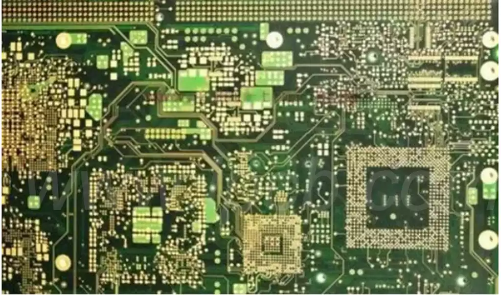
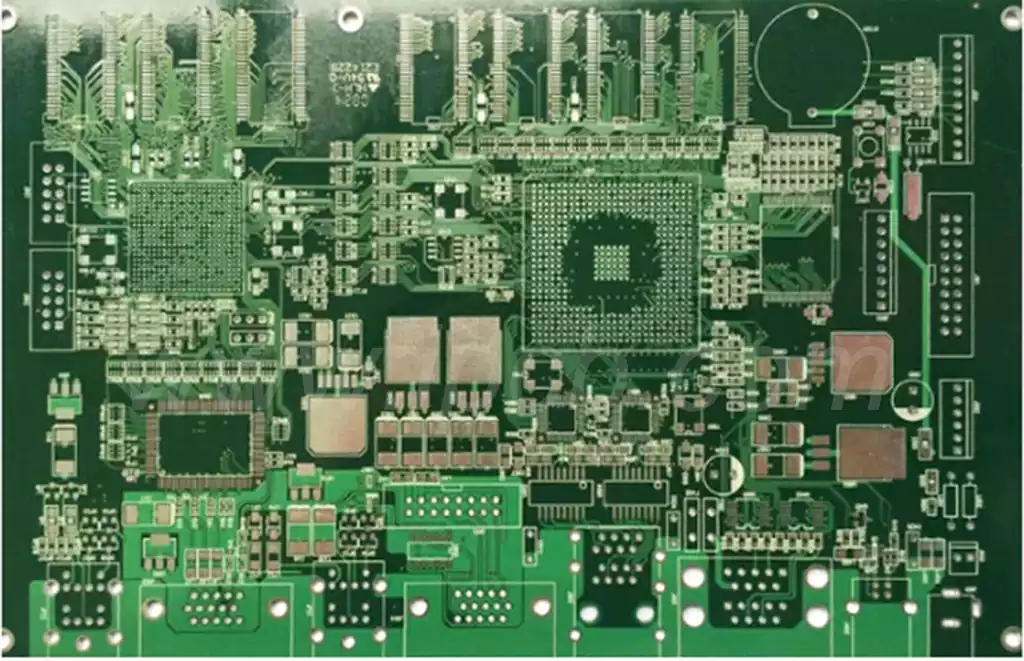
Electroplating copper is the key process of metallization of printed circuit board (printed circuit board, PCB) formation holes, which is an important part of the PCB production process. In order to make the quality and performance of the copper plating layer to meet the PCB requirements, it is often necessary to add some organic additives in the copper plating solution. At present, the most widely used and mature copper plating system in PCB copper plating is the acidic copper sulfate system with copper sulfate and sulfuric acid as the main components.
Acid Electroplating copper principle
Electroplating is the use of chemical electrolysis principle, in a specific metal surface plated on a thin layer of a specific metal or alloy process. Acid copper plating is also called β-anode method of copper plating, plating, plating metal Cu for the anode, the anode Cu gets two electrons to be oxidized into a cation into the plating solution; PCB board for the metal products to be plated as the cathode, the plating solution in the Cu2 + cations in the PCB board Cu metal surface lose two electrons to be reduced to form Cu.
Electroplated copper layer has good electrical conductivity, thermal conductivity and mechanical ductility and other advantages, is the printed circuit board (PCB) manufacturing indispensable key plating technology.
Printed circuit board copper plating has a full plate copper plating, graphic line copper plating and copper plating of microvia production, etc., commonly used plating solution has sulfate plating solution, pyrophosphate straight plating solution and cyanide plating solution, and is more commonly used is acid sulfate plating solution.
PCB copper plating process:
1. Make coppering solution
First prepare a certain proportion of coppering solution, generally composed of copper sulfate, sulfuric acid and hydrochloric acid. Mix copper sulfate and sulfuric acid according to a certain ratio, add enough water, and mix well. Then add hydrochloric acid into the mixture gradually and continue to stir. The final liquid obtained is the coppering solution.
2. Cleaning PCB plate
The made circuit board is cleaned with acetone or other cleaners to remove the surface dirt and oxidized layer. Then rinse it with water and keep it dry.
3.Coating photopolymer
Coat the photopolymer evenly on the copper-plated surface of the PCB board, and use a light shield to cover it. Then put the PCB board in the dryer to make the photopolymer completely dry.
4. Exposure and development
The PCB substrate has been dried with the drawing layer for alignment, the use of exposure machine for exposure. Then the exposure of the PCB board placed in the developing solution, waiting for the developing solution will not be exposed to the photopolymer partially dissolved, showing the copper disk graphics.
5. Copper plating
According to show the copper disk graphics, the PWB board into the coppering solution, copper plating. First chemical copper plating on the PCB board, and then electroplating, so that the copper layer is more solid. According to different needs, multiple copper plating can be performed to obtain a thicker copper layer.
6. Cleaning and trimming
The copper-plated PCB is cleaned with dilute sulfuric acid to remove the oxide layer on the surface. Then trimming, to remove excess copper layer, so that the PCB board on the line more clear.
7.Final Processing
After trimming the circuit board for anti-corrosion treatment to protect the copper layer from oxidation and corrosion.
PCB copper plating layer delamination reasons:
Substrate and copper delamination: If it is a double-sided board, this may be a problem with the supplier of the substrate.
Delamination of plating and copper sinking layers: this is usually due to contaminants such as antioxidants and oils on the underlying copper layer, resulting in delamination of the second layer from the underlying layer.
Separation between the surface treatment layer and the copper layer: The cause is similar to delamination of the plating and copper immersion layers, and treatments usually include a sandblasting process or plasma treatment.
Improper packaging or preservation: e.g. moisture or too long a period of preservation beyond the shelf life.
Supplier material or process problems: It may be a problem with the material or process itself.
Poor design selection and copper surface distribution: Poor distribution of copper surfaces during design may also lead to delamination.
Thermal stress: Delamination may occur due to stress caused by temperature changes.
Soldermask failure: Failure of the soldermask may also lead to delamination.
Poor Manufacturing Process: Problems in the manufacturing process, such as poor plating processes.
Poor quality materials: Poor quality materials are used.
Wrong type of FR-4 Tg material: An unsuitable type of FR-4 Tg material was selected.
Methods to deal with delamination of the copper plating layer may include baking the PCB board to remove moisture, controlling the exposure energy to ensure good bonding of the film to the copper, and adjusting the lamination temperature and pressure to avoid warping and peeling.
Electroplating copper as a key link in the manufacturing of printed circuit boards, its quality and performance for the overall performance of the board has a critical impact. In the actual production process, we need to strictly control the composition and process parameters of the copper plating solution to ensure that the quality and performance of the plating layer to meet the requirements of use.