PCB wiring is a critical step in PCB design, which determines the performance and reliability of the product. It refers to the process of rationally laying out and connecting wires, components, etc. on a circuit board when manufacturing a printed circuit board (Printed Circuit Board, or PCB for short). This process needs to follow certain rules and principles to ensure the performance and stability of the circuit board.
PCB wiring common rules
PCB board pre-divided digital, analog, DAA signal wiring area.
Digital, analog components and the corresponding line as far as possible separate and placed in their respective wiring areas.
High-speed digital signals as short as possible.
Sensitive analog signals should be routed as short as possible.
Reasonable distribution of power and ground.
Separate DGND, AGND, and ground.
Use wide wires for power and critical signal alignments.
Power and ground lines should be radialized as much as possible, as well as signal lines should not have loopback alignments.
Digital circuits are placed near parallel bus/serial DTE interfaces and DAA circuits are placed near telephone line interfaces.
Small discrete device alignment shall be symmetrical, more densely spaced SMT pad leads should be connected from the outside of the pad, not allowed to connect directly in the middle of the pad.
Priority of key signal lines: power supply, touch small signals, high-speed signals, clock signals and synchronization signals and other key signals have priority.
Priority principle of wiring density: from the single board connected to the most complex relationship between the device start wiring. From the single board on the densest area of the line to start wiring.
PCB design should be avoided to produce sharp corners and right angles, resulting in unnecessary radiation, while the PCB board production process performance is not good.
SMD pads can not have through holes, so as to avoid the loss of solder paste caused by component soldering. Important signal lines are not allowed to pass through from pin to pin.
Wiring of the basic essentials
In PCB design, wiring is an important step in the completion of product design, it can be said that the previous preparatory work is done for it, in the whole PCB, to the design process of wiring the highest qualification, the most detailed skills, the largest workload.
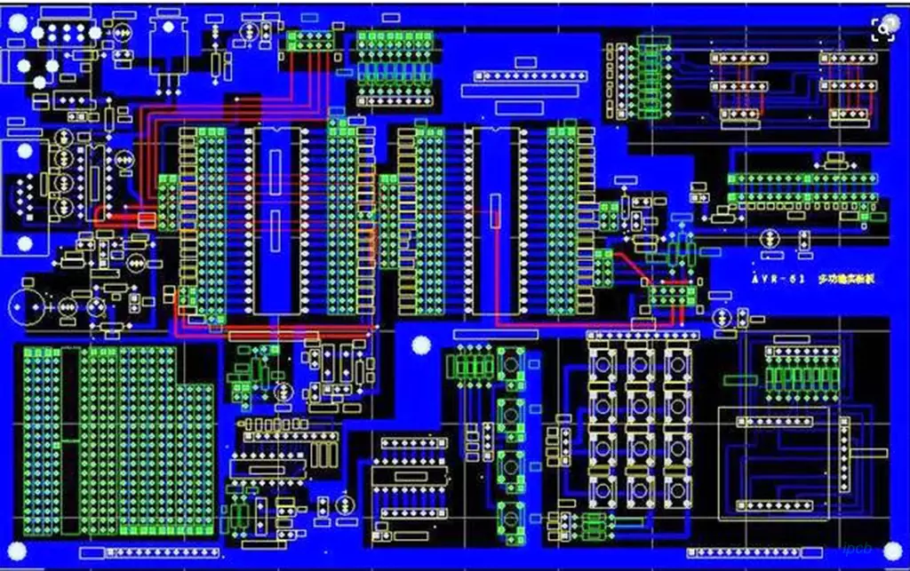
PCB layout has a single-sided wiring, double-sided wiring and multilayer wiring. There are also two types of wiring: automatic wiring and interactive wiring, before the automatic wiring, can be used to interact with the more stringent requirements of the line in advance for wiring, input and output side lines should be avoided adjacent to the parallel, so as not to produce reflective interference. If necessary, ground isolation should be added, the wiring of the two neighboring layers should be perpendicular to each other, parallel is prone to parasitic coupling.
Automatic wiring of the cloth through the rate, depending on a good layout, wiring rules can be pre-set, including the number of bends, the number of holes, the number of steps, and so on. Generally, the first exploratory cloth warp, quickly connect the short line, and then maze wiring, the first to cloth the connecting line for global wiring path optimization, it can be required to disconnect the cloth has been laid line. And try to re-route again to improve the overall results.
The current high-density PCB design has been felt through the hole is not too adaptable, it wastes a lot of valuable wiring channels, in order to solve this contradiction, the emergence of blind holes and buried holes in the technology, which not only completes the role of the guide through the hole, but also save a lot of wiring channels so that the wiring process to complete a more convenient, more fluid, more complete, the PCB board design process is a complex and simple process to be well To master it, but also the majority of electronic engineering designers to experience, in order to get the true meaning of it.
PCB wiring is a precision work, it requires engineers in-depth understanding of the circuit schematic under the premise of carefully designing the wiring path, and clever use of wiring techniques to maximize the performance and stability of the circuit. In addition, engineers also need to continue to accumulate practical experience, and good use of professional tools, so as to achieve better results in the design process.