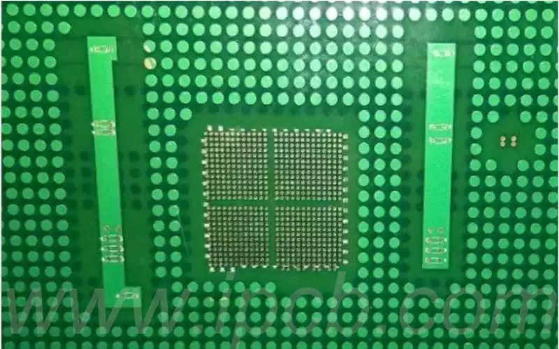
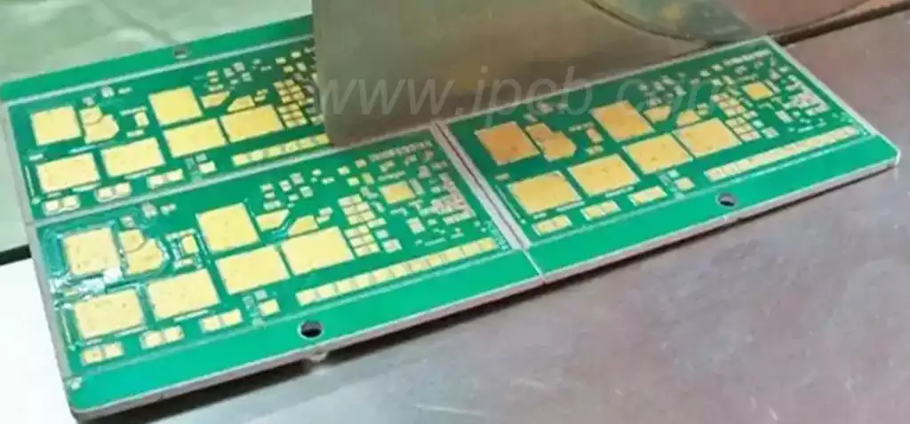
Postage stamp holes are holes with a small diameter and shallow depth, usually about 0.254 mm in diameter and 0.167 mm in depth, and are round or oval in shape, and sometimes in other shapes, such as square, triangle, etc. Stamp holes can be customized to meet specific needs.Postage stamp holes size and shape can be customized according to specific needs to meet different application scenarios.
The role of the postage stamp holes
- Connecting other circuit boards or modules
The main function is for connecting other circuit boards or modules. In some complex electronic products, it is necessary to connect multiple circuit boards or modules together to achieve higher performance and greater functionality. This is where the stamp hole becomes an essential connection. Through this hole, multiple pcb or modules can be connected together to form a complete system. - Improve the reliability and stability of the system
It can also improve the reliability and stability of the whole system. The use of stamp holes is especially important in some occasions where the stability of the system is required to be high, such as aerospace, military and other fields. It can connect the various components together to form a tight whole, thus improving the reliability and stability of the whole system. - Easy maintenance and upgrading
It can also facilitate maintenance and upgrading. In some occasions that require frequent replacement or upgrading, such as industrial automation, medical equipment and other fields, the use of stamp holes is particularly important. It can be easily replaced or upgraded in which parts without disassembling the whole system, thus saving time and cost.
Process Considerations
Plate spacing
The board-to-board spacing during imposition should be in accordance with the process requirements of the plate maker; empirically, the general board spacing is 1.6-2mm.
Hole spacing
As the foot of the daughter board, the spacing between the stamp holes and the stamp holes, and the spacing between the stamp holes and the edge of the pcb board should meet the process requirements of the board-making factory; experience, the spacing between the stamp holes is not less than 0.6mm, and the spacing between the stamp holes and the edge of the board is not less than 1mm.
Hole Size
As a daughter board pins, the hole diameter and hole pad width of the stamp holes should be in line with the process requirements of the board factory; experience, the hole diameter is generally not less than 0.6mm, the hole pad width is generally not less than 0.1mm.
Edge processing
As a sub-board pins, the edge treatment of the stamp hole should meet the process requirements, should be smooth and burr-free. The edges should be chamfered for testing and welding.
Surface Finish
As a daughter board pin, the surface of the stamp hole should be plated with gold (or copper) to improve the mechanical properties of the pad, conductivity, oxidation resistance and easy to tin and solder.
Design requirements
- The number of holes is usually 5 in a group, used to connect components together, may vary depending on the PCB design.
- The size is typically 0.020 inches or 0.5 mm in diameter and may vary depending on the PCB design. PCB postage stamp holes sizes are determined by the thickness of the material used to make the PCB.
- Hole spacing is usually 0.030 inches or 0.76 mm, which prevents components from getting too close together and causing short circuits.
4 PCB postage stamp holes Design Tips
- Enough pull tabs to maintain the PCB
Since the PCB postage stamp holes is an opening, which means that there is no connection between the two, if this is the case, a short circuit can occur between the two parts of the PCB.
In order to avoid this from being released, it is necessary to make sure that the tabs are strong enough to support the weight of the components above them.
- Should be kept away from sensitive pcb components
It is necessary to stay away from sensitive components because the pull tabs are easily damaged and can easily lead to an electrical short circuit. - The spacing between the two stamp holes should be between 60mm-90mm
If the space between two stamp holes is too large, it is not convenient to install components. If the spacing is too small, the solder will easily flow to other places and cause short circuit. - At least 0.125ich spacing between the nearest components
There should be at least 0.125 inches of clearance between the nearest components, especially for high-density PCBs. the closer the components, the more difficult it will be to fix the solder. Too close and solder bridges tend to form between pads/alignments.
Advantages:
- Better strength, can be broken right off, unlike taps that require milling equipment to cut them
- Have a greater grip, the larger the hole, the larger the surface area of the adhesive to catch, so that the installation will be easier, and can prevent PCB movement.
Postage stamp holes,as an important element in PCB design,ensure the stability and reliability of electronic products with its unique connection function and process requirements.