As electronic devices accelerate toward miniaturization, higher power, and higher operating frequencies, unprecedentedly stringent requirements are being placed on circuit board precision, thermal performance, and reliability. Ceramic circuit boards, benefiting from their inherent material advantages, have become a core choice for high-end applications. Among the various manufacturing approaches, the DPC (Direct Plated Copper) process has emerged as a key technology that overcomes the challenges of producing high-precision ceramic circuit boards. How does this process achieve micron-level circuit patterning, and why has it become a mainstream solution for high-end ceramic substrates? This article provides an in-depth analysis of the technical principles, core advantages, and application value of the DPC process, revealing the manufacturing logic behind high-precision ceramic circuit boards.
Core Principles of the DPC Process
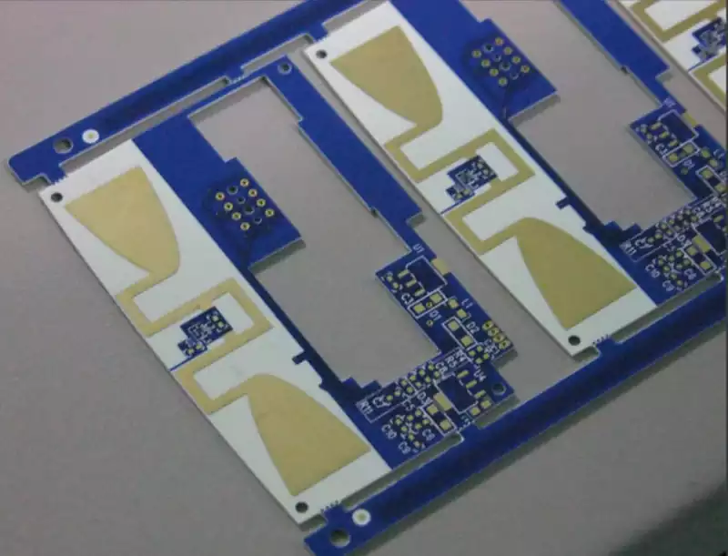
DPC, short for Direct Plated Copper, is based on the concept of bypassing traditional intermediate metallization layers used in ceramic circuit board fabrication. Through a combination of chemical and physical processes, copper is directly deposited and firmly bonded onto the ceramic substrate surface, forming high-precision metal circuitry. Compared with thick-film printing or AMB brazing processes, the defining characteristic of DPC is “direct formation.” It does not rely on paste sintering or brazing fillers, fundamentally improving circuit accuracy and interfacial bonding stability.
The complete DPC process consists of seven critical steps, each requiring strict parameter control. The first step is ceramic substrate pretreatment. Alumina, aluminum nitride, or other ceramic substrates undergo precision grinding, cleaning, and surface activation to remove contaminants and oxide layers while creating a micro-roughened surface to enhance copper adhesion. The second step is seed layer deposition. Using sputtering or evaporation, an ultra-thin titanium/copper seed layer—typically 50–200 nm thick—is deposited on the ceramic surface. The titanium layer serves as an adhesion-promoting transition layer, while the copper layer provides a conductive base for subsequent electroplating.
The third step involves photoresist coating and exposure. Liquid photoresist is uniformly applied over the seed layer and thermally cured, then exposed to ultraviolet light through a high-precision photomask, causing a photochemical reaction in the circuit pattern areas. The fourth step is development and etching. Specialized developer solutions remove unexposed photoresist, exposing the seed layer where copper deposition is required, followed by etching to remove unwanted seed layer regions. The fifth step is electroplating thickening. The substrate is immersed in a copper sulfate plating bath, where copper ions deposit and grow on the exposed seed layer under precisely controlled current density, temperature, and time, forming metal traces with thicknesses ranging from 10 to 100 μm. The sixth step is photoresist stripping and seed layer removal, eliminating remaining photoresist and etching away residual seed layers outside the circuit pattern. The final step involves post-processing, including surface passivation, cleaning, drying, and quality inspection to ensure compliance with performance requirements.
The core strengths of this process lie in its “directness” and “precision.” Because bonding between the seed layer and plated copper does not require high-temperature sintering, thermal stress-induced deformation or cracking of the ceramic substrate is avoided. The combination of photolithography and electroplating enables minimum line width and spacing below 50 μm, far exceeding the 100 μm limit of thick-film printing, thereby meeting the demands of high-density packaging.
Key Advantages of the DPC Process
The DPC process stands out in high-end ceramic circuit board manufacturing due to its comprehensive advantages in precision, performance, and reliability, which align closely with the core requirements of advanced electronic equipment.
Circuit precision and density are the most prominent strengths of DPC. Through the synergy of photolithography and electroplating, micron-level circuit patterning can be achieved, with minimum line width/spacing reaching 30/30 μm, and even 20/20 μm with advanced equipment. This high precision enables ceramic circuit boards to integrate more circuits and components, supporting device miniaturization and high-density packaging. In contrast, thick-film printing is limited by paste particle size and printing accuracy, making it difficult to reduce line widths below 100 μm, which restricts its suitability for high-frequency and high-density applications. Although AMB can achieve finer patterns, its process complexity and cost are significantly higher.
In terms of thermal performance and bonding stability, the DPC process also delivers outstanding results. Since copper is directly deposited onto the ceramic substrate without unnecessary intermediate layers, heat can be efficiently transferred through the copper traces into the ceramic substrate and dissipated. For aluminum nitride substrates, DPC-fabricated boards can maintain thermal conductivity levels of 150–200 W/(m·K), approaching the intrinsic thermal performance of the ceramic itself. This effectively addresses heat dissipation challenges in high-power devices. At the same time, the strong bonding between the seed layer and electroplated copper ensures excellent adhesion. After thermal cycling and thermal shock testing, trace delamination rates are significantly lower than those observed with thick-film processes, resulting in longer service life.
The DPC process also offers excellent compatibility and flexibility. It can be applied to various ceramic substrates, including alumina, aluminum nitride, and zirconia, to meet diverse performance requirements. Circuit thickness can be flexibly adjusted from 10 μm to 100 μm by controlling plating time, enabling customized current-carrying capacity. In addition, DPC supports irregularly shaped substrates and multilayer circuit designs, further expanding the application scope of ceramic circuit boards.
Technical Challenges of the DPC Process
The high precision and performance of the DPC process are achieved through overcoming multiple technical challenges, which also explain the higher R&D and manufacturing investment required for DPC-based ceramic circuit boards.
Ceramic substrate pretreatment represents the primary challenge. Ceramics are inherently hard, brittle, and chemically stable, with smooth surfaces that hinder adhesion. Inadequate pretreatment can significantly reduce bonding strength between the seed layer and the substrate, leading to copper peeling or blistering during electroplating. Therefore, grinding precision must be carefully controlled to create a uniform micro-roughened surface, while activation treatments enhance surface reactivity. These steps demand extremely high equipment accuracy and process control. Moreover, different ceramic materials—such as alumina and aluminum nitride—exhibit distinct physical and chemical properties, requiring tailored pretreatment solutions and increasing process complexity.
Seed layer deposition and electroplating parameter control are equally critical. Uniform seed layer thickness directly affects the quality of subsequent copper plating. Non-uniform thickness can result in uneven copper deposition rates, causing variations in trace width and edge burrs. Consequently, sputtering or evaporation equipment must provide excellent vacuum stability and uniformity control, typically maintaining thickness deviation within ±5 nm. During electroplating, even minor fluctuations in current density, bath temperature, or pH can influence copper crystallization quality and adhesion strength. High-precision sensors and automated control systems are therefore required for real-time monitoring and adjustment, placing stringent demands on equipment automation and stability.
Photolithography and development accuracy is the foundation of micron-scale patterning. Photomask precision must reach sub-micron levels, as any deviation can distort circuit patterns. Photoresist coating thickness must be uniform to ensure consistent exposure results. During development, parameters such as developer concentration, temperature, and immersion time must be precisely controlled—insufficient development can leave residues, while overdevelopment may damage the seed layer. Coordinating these variables is extremely challenging and requires extensive process experience and rigorous quality control systems.
Yield control presents another challenge. Due to the brittle nature of ceramic substrates, cracking or breakage may occur during pretreatment, photolithography, or electroplating. As circuit precision increases, the risk of defects such as shorts and opens also rises. Currently, industry-wide DPC yields typically range from 80% to 85%, higher than those of AMB processes but lower than the over-95% yields common in conventional PCB manufacturing. The material and processing costs of rejected units further elevate overall manufacturing costs.
Application Scenarios of the DPC Process
Thanks to its high precision, excellent thermal performance, and superior reliability, DPC-based ceramic circuit boards are widely used in multiple high-end manufacturing sectors and have become indispensable core components.
In the semiconductor and microelectronics field, DPC ceramic circuit boards are ideal for power device packaging. Power devices such as IGBTs and MOSFETs generate substantial heat during operation while packaging space continues to shrink, requiring circuit boards that combine high circuit precision with efficient heat dissipation. DPC-fabricated ceramic circuit boards support high-density circuit layouts and rapid heat transfer, reducing junction temperatures and enhancing device stability and lifespan. They are widely used in new energy vehicle power control systems, industrial inverters, and photovoltaic inverters.
Aerospace and defense applications impose extremely high demands on reliability and environmental adaptability. DPC ceramic circuit boards, with their excellent radiation resistance, high-temperature tolerance, and vibration resistance, serve as core components in these fields. In satellite communications, airborne radar, and missile guidance systems, DPC-based boards can operate reliably under extreme temperatures ranging from −55°C to 125°C, strong radiation, and intense vibration, ensuring stable system performance.
High-end medical equipment is another important application area. Medical imaging systems such as CT and MRI scanners, as well as laser therapy equipment, require exceptional precision and stability from electronic components. DPC ceramic circuit boards enable high-precision signal transmission while efficiently dissipating heat, preventing performance degradation due to overheating and ensuring diagnostic and therapeutic accuracy. In implantable medical devices, the high reliability of DPC technology further reduces failure risks and enhances patient safety.
The DPC direct plated copper process, with its distinctive technical logic, has successfully addressed the manufacturing challenges of high-precision ceramic circuit boards, providing critical support for the advancement of high-end electronic equipment. Its micron-level circuit accuracy, excellent thermal performance, and reliable bonding stability precisely match the demanding requirements of industries such as new energy, aerospace, and medical technology. At the same time, the technical challenges associated with DPC continue to drive ongoing process optimization and equipment upgrades across the industry.
As electronic devices continue to demand higher precision and performance, the application scope of the DPC process will continue to expand. Parallel efforts to improve yield and reduce cost are also expected to intensify. Looking ahead, advances in photolithography, electroplating equipment, and ceramic materials are likely to enable even higher circuit precision, lower manufacturing costs, and greater production efficiency, further promoting the adoption and application of high-precision ceramic circuit boards.