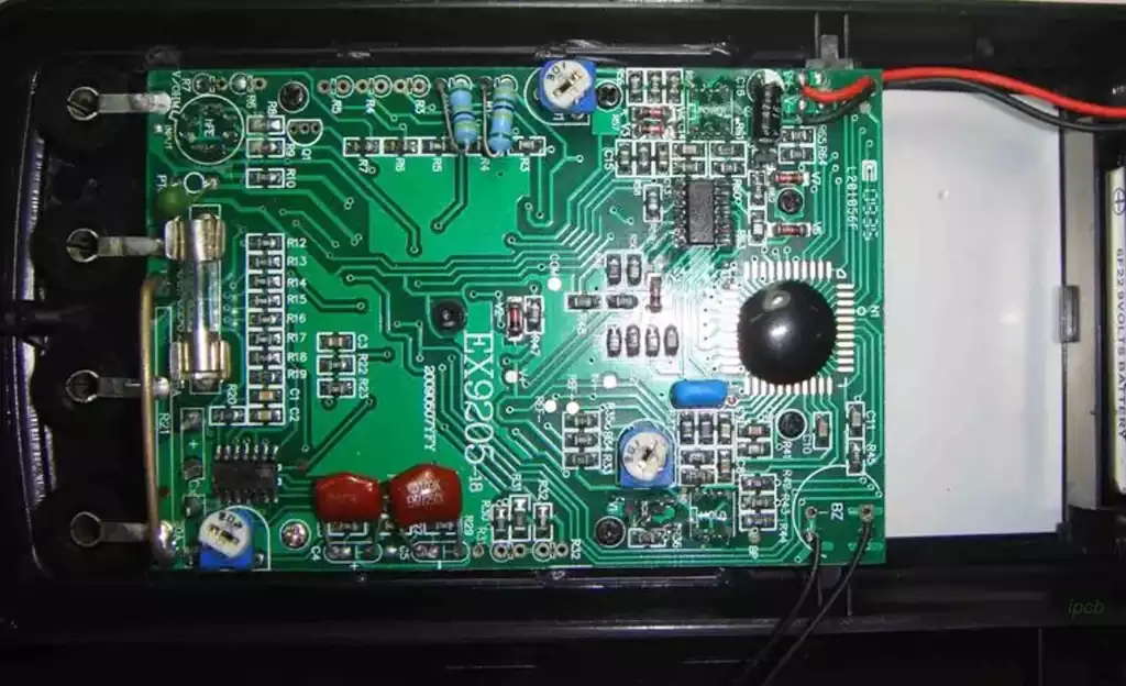
In antenna PCB design, electromagnetic compatibility (EMC) is a key factor in ensuring stable device performance and minimizing interference. As core elements of EMC design, layout and routing are not only cost-effective but also provide the most direct and efficient means of improving EMC performance.
Unlike conventional PCB routing, antenna PCB routing must balance antenna radiation performance with electromagnetic interference suppression, preventing unwanted coupling caused by improper layout.
Layout and routing are central to EMC optimization in antenna PCB and represent the lowest-cost, most immediately effective design measures. The essential difference between antenna circuit board routing and standard PCB routing lies in the need to simultaneously consider radiation efficiency and interference control.
The core principle of layout optimization is “isolation.” By strategically arranging components, spatial coupling between interference sources and the antenna can be minimized. For high-frequency digital circuits and antennas, sufficient safety spacing must be maintained. Typically, the distance between an antenna and clock circuits above 100 MHz should not be less than one-quarter of the wavelength. For example, a 2.4 GHz antenna should be at least 31 mm away from high-frequency digital circuits. The distance between the antenna and power modules such as DC-DC converters or LDO regulators should be no less than 20 mm to prevent power noise from coupling into the antenna through radiation.
In multi antenna pcb designs, antennas operating in the same frequency band should be spaced at least half a wavelength apart, while antennas operating in different frequency bands should be separated by at least one-quarter of the lowest operating wavelength. This helps control mutual coupling within an acceptable range. In addition, the main radiation lobe of the antenna should face outward from the device enclosure, while digital circuits and power modules should be positioned toward the interior to further reduce cross-radiation interference.
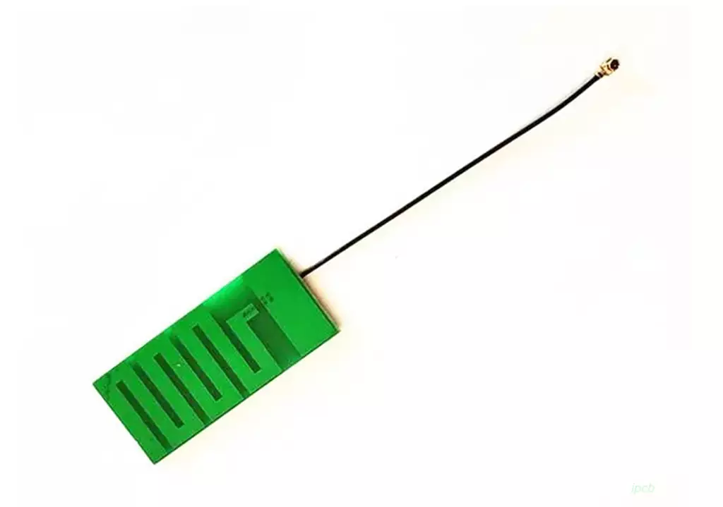
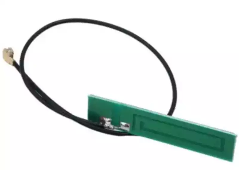
The key to routing design is “standardization.” Poor routing can easily create unintended radiation sources. The antenna feed line, as the critical signal transmission path, must maintain a strict characteristic impedance of 50 Ω (the standard impedance in most RF systems). The entire transmission path from the RF chip to the antenna connector must remain impedance-matched to minimize signal reflection and associated interference. Feed lines should be short and straight, avoiding right-angle bends and unnecessary branches.
Corners should use 45° angles or curved transitions to prevent impedance discontinuities that may cause radiation. Power traces should be spaced at least 10 mm away from antenna feed lines, and parallel routing should be avoided. If unavoidable, the parallel length should be limited to less than 5 mm to reduce conductive coupling.
In addition, differential signal routing can significantly enhance interference immunity, especially for sensitive signal transmission. Differential pairs should follow equal-length, equal-spacing, and symmetrical routing principles. The length mismatch should be controlled within 127 μm, and spacing must remain consistent to leverage common-mode noise suppression and reduce crosstalk. High-frequency signal traces should maintain a continuous ground plane beneath them to provide a proper return path, reduce ground bounce noise, and prevent loop antenna effects that increase electromagnetic radiation.
Grounding design should focus on “low impedance and no loops.”A continuous ground plane forms the foundation of EMC performance. Antenna PCB are recommended to use a solid, uninterrupted ground plane, avoiding slots or splits that could lengthen return paths and increase impedance.In mixed analog-digital circuits, analog and digital grounds should be connected at a single point near the power entry to prevent ground loops.
This connection point should be kept away from sensitive analog circuits and antenna feed networks to minimize interference caused by ground potential differences. Antenna ground pins should be connected to ground as close as possible, with short return paths and ground impedance controlled below 0.1 Ω to ensure stable radiation performance and reduced emissions.
Shielding design should be selected according to interference intensity and application requirements, balancing shielding effectiveness with product miniaturization. For strong interference sources such as DC-DC modules and high-frequency clock circuits,metal shielding enclosures (aluminum or brass, 0.2–0.3 mm thick) can be used. The shielding enclosure must be reliably soldered to the ground plane to ensure shielding effectiveness of at least 40 dB at the operating frequency band. If heat dissipation is required, ventilation holes may be added, with diameters no greater than one-twentieth of the wavelength to prevent degradation of shielding performance.
For sensitive antennas such as GPS antenna or millimeter-wave radar antennas, a ground via array (0.3 mm diameter, 0.5 mm spacing) combined with a metal shielding frame can be placed around the antenna to form an electromagnetic barrier, reducing external interference by more than 30 dB. Care must be taken to ensure that shielding structures do not degrade antenna radiation performance; the spacing between the shielding frame and the antenna must be carefully controlled to avoid reduced radiation efficiency.
Filtering design is essential for blocking conducted interference. By adding filtering components at power and signal interfaces, interference propagation can be suppressed, complementing layout, grounding, and shielding strategies to form a comprehensive EMC protection system. Power filtering should adopt a multi-stage approach.
A π-type filter can be added at the RF chip power input, consisting of a series RF choke and parallel electrolytic and MLCC capacitors, to suppress power noise in the 100 kHz–1 GHz range with noise attenuation of at least 30 dB. An EMI filter at the system power entry point can further suppress common-mode and differential-mode interference from the mains supply to ensure conducted emissions compliance.
Signal line filtering should be implemented selectively. Ferrite beads can be placed in series with digital signal lines connected to the antenna PCB to suppress digital noise conduction. Attenuators or isolators may be inserted between the antenna feed line and the RF chip to reduce chip-generated noise coupling into the antenna and to limit interference signals received by the antenna from entering the chip. The selection of filtering components must match the antenna’s operating frequency band to ensure that signal transmission performance is not compromised, maintaining both radiation efficiency and EMC compliance.
EMC design for antenna PCB is a systematic engineering process. It requires coordinated optimization of layout, routing, grounding, shielding, and filtering to achieve a balanced integration of antenna radiation performance and electromagnetic interference suppression.