The soundness of RF board layout directly determines the transmission quality of RF signals, interference immunity and the overall performance of the equipment; it is a core aspect of RF product design. This article focuses on its core principles, preparation, practical implementation and simulation, outlining key points to guide engineering practice.
Core Principles of RF Board Layout
Minimise transmission paths: The shorter the traces carrying RF signals (particularly those at ≥1 GHz), the lower the loss and radiation. Redundant traces and unnecessary vias are strictly prohibited; priority should be given to ensuring straight paths.
Strict impedance control: The standard impedance for RF traces is 50 Ω (general) or 75 Ω (specific scenarios); impedance tolerance must be kept within 5%, which is stricter than the requirements for high-speed digital boards.
Clean Ground Reference: RF grounds must be low-impedance and unbroken, ensuring short and continuous signal return paths to eliminate interference caused by ground loops.
Shielding and Isolation: RF circuits operating at different frequencies or power levels (e.g., transmit/receive channels, PA/LNA) must be physically isolated to prevent mutual interference and ensure signal purity.
Preliminary Preparation: Laminate and Board Selection
RF Board Selection (Prioritising High-Frequency Characteristics)
The key considerations for RF board selection are the stability of the dielectric constant (Er) and dielectric loss (Df), whilst balancing cost and heat dissipation requirements. The specific classifications are as follows:
Low-frequency RF (<3 GHz): High-frequency modified FR-4 (e.g. Isola FR408HR, Er=3.7, Df≤0.008) may be selected; this offers controllable costs and meets basic requirements.
High-frequency RF (3 GHz–28 GHz): Specialised low-loss materials must be selected to minimise signal attenuation. Commonly used types include Rogers RO4350B (Er = 3.48, Df = 0.0037) and PTFE-based materials (e.g. Taconic TLY-5, Er = 2.2).
Additional key parameters: The dielectric constant must vary minimally with frequency and temperature to ensure impedance stability; for high-power RF modules, attention must be paid to the thermal conductivity of the substrate to improve heat dissipation efficiency.
Layer-by-layer design (prioritising RF layers with a reference ground)
Single/double-layer RF boards (simple circuits, such as Bluetooth modules): RF traces are routed on the top layer, with a complete ground plane laid on the bottom layer; the spacing between the top and bottom layers is ≤0.2 mm, forming a microstrip structure that facilitates precise impedance control.
Multi-layer RF boards (complex circuits, such as 5G base stations): At least one complete ground plane (GND) must be reserved as the RF signal reference layer; the spacing (H) between the RF traces and the GND layer must be precisely calculated (as this directly affects impedance values);
The power supply layer and ground layer must be tightly coupled (spacing 0.1 mm) to reduce power supply noise interference with the RF signal;
RF signal layers must not be adjacent to digital signal layers, and must be isolated by a ground layer in between to prevent crosstalk.
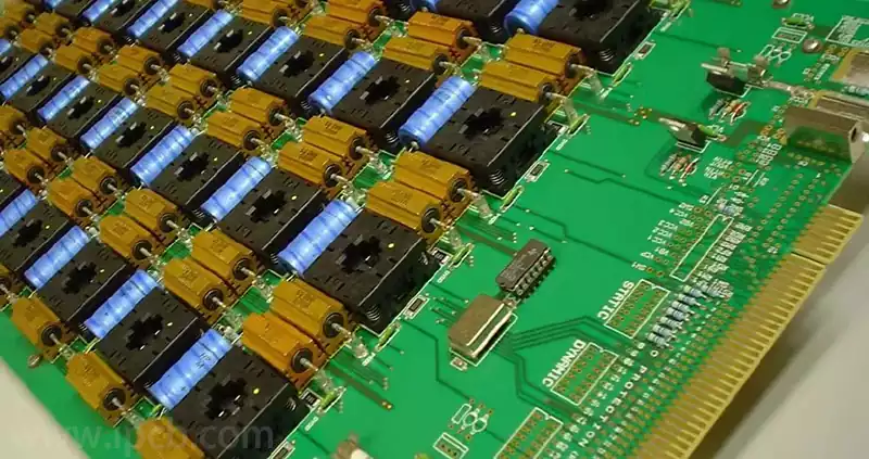
Layout Guidelines for Key RF Board Components
Layout according to signal flow: RF front-end components must be arranged in the following sequence: ‘antenna interface → filter → LNA/PA → mixer → baseband’. Avoid signal path crossings and detours. Example: antenna connector → duplexer → power amplifier (PA) → transceiver chip. Ensure the path is as short and straight as possible.
Isolation of Sensitive Components: A spacing of ≥20 mm must be maintained between high-power devices (PA, power inductors) and low-noise devices (LNA, RF switches). Where necessary, use a metal shielding enclosure to prevent high-power interference with low-noise signals.
Keep Clock Sources Away from RF Paths: Clock sources such as crystal oscillators and voltage-controlled oscillators (VCOs) must be kept away from RF traces to prevent their harmonics from interfering with RF signals.
Ground Pad Design: The exposed pads on RF chips (e.g., PAs) must be connected directly to the ground plane via four ground vias with a diameter of 0.3 mm to minimise thermal resistance and ground impedance; the ground leads of capacitors and inductors must be short and wide, with ground vias placed as close as possible, with a distance from the lead of ≤1 mm.
Core Specifications for RF Board Routing
RF Transmission Line Design (Impedance and Structural Matching)
Select the appropriate transmission line type based on the application scenario, with a focus on controlling impedance consistency, as detailed below:
Microstrip: Top-layer RF trace + bottom-layer ground plane. Suitable for most RF scenarios, offering ease of fabrication and simple impedance calculations. The relationship between trace width (W) and dielectric thickness (H) can be calculated using tools such as Allegro or Polar. For example, a 50Ω microstrip on RO4350B (H=0.254mm) board requires a trace width of approximately 0.3mm.
Stripline: The RF trace is sandwiched between two ground planes, offering excellent shielding and suitability for high-interference environments; loss is slightly higher than that of microstrip.
Coplanar waveguide (CPW): Ground planes are present on both sides of the RF trace; suitable for millimetre-wave (≥30 GHz) applications; strict control of trace width and side-to-ground spacing is required.
Routing Specifications
Bend Treatment: Right-angle bends are prohibited; use 135° angles or curved transitions with a radius of curvature ≥ 3 times the trace width to avoid sudden changes in impedance and signal reflection.
Trace Width Control: The width of RF traces must remain consistent throughout; sudden widening or narrowing is strictly prohibited. If a transition is absolutely necessary, the transition length must be ≥ 10 times the difference in trace width.
Spacing Requirements: RF traces must be positioned at least 5 mm from the board edge to prevent edge radiation; spacing from other signal traces must be at least 5 times the trace width to minimise crosstalk.
Via and Connector Design (Minimising Parasitic Parameters)
RF Vias: Prioritise blind or buried vias, or back-drilled vias (with excess stubs removed) to reduce parasitic inductance (through-hole parasitic inductance is approximately 0.5–1 nH, which can severely affect high-frequency signals); Via diameter: 0.3–0.5 mm; pad diameter: twice the via diameter; surround with 3–4 ground vias (forming a ‘ground moat’) to shorten the signal return path.
RF Connectors: For connectors such as SMA and MCX, the connector housing must be soldered directly to the ground plane; the centre pin trace must maintain impedance continuity with the RF line, and an impedance transition must be provided at the pins; no signal lines are permitted beneath the connector, and the bottom layer must be a complete ground plane.
Layout of matching networks (capacitors, inductors, resistors)
Components in RF matching circuits (such as π-type or T-type matching) must be laid out compactly, with the following core requirements:
Component spacing ≤ 2 mm, forming a “compact network” to reduce interference from parasitic parameters.
Component leads should be kept as short as possible, with pad dimensions matching the component package (e.g., 0.8 mm long and 0.4 mm wide for a 0402 package), to avoid parasitic capacitance caused by excess copper.
The ground terminals of matching components must be connected directly to the ground plane via vias; “wire-to-ground” connections are strictly prohibited to ensure reliable grounding.
Ground and Shielding Design (Core of Interference Prevention)
Ground Plane Design
The ground plane in the RF area must not be segmented; digital ground and RF ground must employ single-point grounding (e.g., via a 0Ω resistor or ferrite bead at the power supply input), to prevent digital noise from entering the RF ground and contaminating the RF signal.
The ground plane copper thickness must be ≥1 oz (35 µm) to enhance conductivity and heat dissipation; in high-power areas (e.g., beneath the PA), 2 oz copper may be used, with additional heat dissipation vias (0.5 mm diameter, 2 mm pitch) to improve heat dissipation.
Shielding Enclosure Design
For critical modules such as transmit/receive channels and PAs/LNAs, use metal shielding enclosures (e.g. nickel silver) for isolation. Specific requirements:
The height of the shielding enclosure must be ≥ (maximum component height + 0.5 mm) to ensure components are not compressed and shielding is effective.
The base of the shielding enclosure must be tightly soldered to the ground plane, with a solder joint every 1 mm, to ensure electromagnetic sealing and prevent interference leakage.
Interference Prevention Details
No openings are permitted in the ground plane beneath RF traces to avoid impedance discontinuities; openings in other areas must be located at least 10 mm away from RF paths.
Power supply traces (e.g., PA power lines) must be thick and short. Multiple decoupling capacitors (10 μF electrolytic capacitor + 0.1 μF ceramic capacitor) should be connected in parallel near the chip’s power pins to filter out power supply noise and prevent interference with RF signals.
Simulation and Verification (Ensuring Layout Compliance)
Pre-layout simulation (optimisation prior to layout)
Use ADS, HFSS or Allegro SI software to simulate the RF board link, focusing on verifying the following parameters:
Impedance matching: S11 (return loss) ≤ -15 dB, with an ideal value of ≤ -20 dB.
Insertion Loss (S21): Loss should be as low as possible within the operating frequency band (e.g., for the 28 GHz band, loss on a 10 cm microstrip line ≤ 1 dB).
Isolation: S21 between transmit and receive channels ≤ -40 dB, to prevent crosstalk from affecting signal quality.
Post-Simulation (Verification after Layout)
Once the layout is complete, extract the transmission line models and via parasitic parameters to simulate signal integrity under actual operating conditions. Focus on optimising areas where reflections or losses exceed specifications to ensure compliance with design requirements.
Testing and Verification (Post-Production Validation)
Upon completion of production, verify performance through the following tests:
Test the S-parameters of the RF ports using a network analyser (e.g., Keysight N9923A) to confirm consistency with simulation results.
Test EMI emissions in a 3m anechoic chamber to ensure compliance with relevant industry standards such as FCC and CE, and to prevent excessive electromagnetic interference.
RF board layout must strictly adhere to all specifications, balancing theory with practical application and paying close attention to every detail. By combining simulation with actual testing for optimisation and adjustment, it is possible to design RF circuit boards that are stable in performance and compliant with standards.