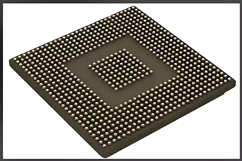
A BGA substrate (Ball Grid Array Substrate) is the core carrier of a ball grid array package; essentially, it is a high-density interconnect (HDI) multilayer PCB used to mount the chip, provide electrical interconnection between the chip and the motherboard, and offer mechanical support, with solder bumps arranged in an array on the reverse side.
Core Structure and Functions of a BGA Substrate
Chip side (front): Features pads and traces, connected to the chip via wire bonding or flip chip mounting.
Intermediate Layers: Multiple layers of conductive patterns and insulating media, including power and ground planes, impedance-controlled traces, and microvias, responsible for signal distribution, power integrity and thermal management.
Package Side (Back): Solder balls are placed in a grid array (e.g. 1.0mm/1.27mm pitch) for surface-mount technology (SMT) mounting onto the motherboard.
Common materials for BGA substrates
Organic resin substrates (such as FR-4, BT resin and ABF resin) are the most widely used. FR-4 is lower in cost and offers good mechanical strength, but has a higher coefficient of thermal expansion, which may cause stress during thermal cycling. ABF resin, on the other hand, is suitable for high-frequency applications, providing superior impedance control—which is crucial for modern 5G and automotive electronics.
Ceramic substrates (aluminium oxide, aluminium nitride, silicon carbide) excel in thermal management. For example, aluminium nitride has a thermal conductivity 5–10 times that of FR-4, making it highly suitable for high-power ICs. However, its high cost means it is typically reserved for specialised applications such as industrial sensors.
Silicon and glass substrates are less commonly used, but their adoption in high-end applications is steadily increasing. Silicon substrates match the thermal expansion coefficient of the chip, thereby reducing stress; glass substrates, meanwhile, offer excellent flatness—a key requirement for ultra-fine-pitch FC-BGA substrate design.
Differences between BGA substrates and standard PCBs
Higher precision: line width/spacing ≤25μm, micro-vias (≤100μm), HDI (High-Density Interconnect).
Specialised materials: BT resin, ABF, LCP, ceramics, etc., featuring low Dk/Df, high heat resistance and low moisture absorption.
More layers: typically 4–16 layers, including dedicated power and ground planes.
Ball placement process: High-precision ball placement is required on the reverse side (solder ball diameter 0.3–0.8 mm).
Core application areas of BGA substrates
The application of BGA substrates is closely linked to the integration level and performance requirements of electronic devices, covering multiple sectors such as consumer electronics, automotive electronics and industrial control.
Consumer electronics is the largest market for BGA substrates. CPUs, GPUs and RF chips in smartphones, tablets and laptops widely utilise BGA packaging; high-end smartphone processors and RF modules predominantly use FC-BGA substrates, whilst power management chips in mid-to-low-end devices are often paired with standard FR-4 BGA substrates. Due to space constraints, wearable devices tend to utilise rigid-flex BGA substrates.
Demand in automotive electronics is growing rapidly. Chips for autonomous driving, in-vehicle infotainment systems and power management require extremely high levels of reliability and thermal stability; consequently, BGA substrates made of ceramic or ABF resin are frequently used to withstand the complex in-vehicle environment, including extreme temperatures and vibration.
The industrial control and server sectors demand high density and reliability. Chips in industrial sensors and PLC controllers commonly use ceramic BGA substrates or high-heat-resistant BT resin substrates; whereas CPUs and memory chips in servers and data centres primarily utilise FC-BGA carrier boards with eight or more layers to meet the demands of high-frequency, high-speed signal transmission.
High-end sectors such as aerospace and medical electronics impose even more stringent requirements on weight, volume and reliability. Aerospace equipment predominantly uses lightweight, highly stable silicon or glass substrate BGAs; medical electronics must meet biocompatibility requirements and typically employ low-moisture-absorption, highly reliable BGA substrates.
Core Manufacturing Processes for BGA Substrates
1.Preparation of the substrate base material
This is the fundamental step that determines the performance of BGA substrates.
Organic resin substrates (e.g. FR-4, BT resin, ABF resin): First, the resin is combined with glass fibre to form a core board, which is then laminated on both sides with extremely thin (12–18 μm) copper foil. This ensures a strong bond between the copper foil and the core board, laying the foundation for subsequent wiring.
Ceramic Substrates: Ceramic powders (such as aluminium oxide or aluminium nitride) are mixed and moulded, then sintered at high temperatures to form a ceramic substrate, which is subsequently metallised to ensure electrical and thermal conductivity.
FC-BGA Substrates: The core technology involves using an ABF film as the substrate material. Through a lamination process, the ABF film is bonded to the core board, providing support for the routing of ultra-fine circuits.
2.Drilling and Via Plating
Precision drilling equipment is used to create microscopic vias (typically ranging from a few micrometres to several tens of micrometres in diameter) in the substrate, which are used to connect the circuits across the substrate’s layers. The drilling accuracy directly impacts the subsequent signal quality. Once drilling is complete, the through-holes undergo metallisation (such as electroless copper plating or electroplating) to ensure good electrical conductivity and prevent poor contact or signal attenuation—this step is also crucial for ensuring the reliability of the substrate.
3.Circuit Formation and Patterning
Through photolithography and etching processes, predetermined circuit patterns (such as conductive traces, electrodes, and pad arrays) are formed on the copper foil surface of the substrate . The width and spacing of the circuits are determined by the substrate’s required routing density; for high-density FC-BGA substrates, line widths can be as small as a few micrometres. Once the patterning is complete, a cleaning process is required to remove photoresist and etching residues, ensuring clear circuits and good electrical conductivity.
4.Solder Mask and Surface Treatment
A solder mask is applied to the substrate surface, exposing only the pads and electrodes required for soldering. The mask protects the circuits from environmental factors such as moisture and dust, and prevents bridging and short circuits during soldering. Surface treatment typically involves processes such as gold plating or nickel plating to enhance the pads’ resistance to oxidation and improve soldering reliability, laying the foundation for subsequent ball attachment and chip bonding.
5.Cutting, Inspection and Packaging
The completed multi-panel substrate (typically containing multiple BGA substrates on a single carrier) is separated into individual substrates using precision cutting equipment; care must be taken during the cutting process to avoid warping or damage to the substrates. A comprehensive inspection is then carried out, covering parameters such as circuit continuity, insulation, dimensional accuracy and warpage, with non-conforming products being rejected. Qualified products are vacuum-packed to prevent moisture absorption or damage, and are finally stored in the warehouse, ready for subsequent packaging use.
With the continuous advancement of 5G, AI and high-performance computing, BGA substrates are evolving towards finer line widths, greater numbers of layers and superior materials. Although they have never attracted as much attention as chips, they remain an indispensable, yet invisible, cornerstone of semiconductor packaging.