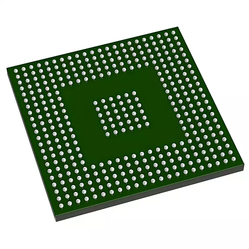
BGA packaging has become the mainstream form of integrated circuit packaging due to its high density, high reliability and excellent electrical and thermal performance. Compared to traditional DIP and QFP packages, BGA distributes solder balls evenly across the underside of the package, resolving the issue of bridging between closely spaced pins, shortening lead lengths, reducing inductance, and enhancing high-speed signal transmission performance.
At the same time, it offers superior thermal conductivity, efficiently transferring heat from the chip to the PCB and preventing damage caused by overheating. As electronic devices evolve towards miniaturisation and higher integration, correct design specifications and defect prevention have become key to ensuring the reliability of BGA packaging.
Key Points in BGA Packaging Design
1.Pitch and Specification Design
The pitch of a BGA package (i.e. the centre-to-centre distance between solder balls) is the most fundamental design parameter; it directly affects packaging density and the difficulty of subsequent assembly. Currently, BGA packages with a pitch of 0.05 to 0.06 inches (approximately 1.27 mm to 1.52 mm) are the most widely used, as this specification strikes a good balance between package density and manufacturability, delivering significant practical benefits. As integration requirements continue to rise, BGA packages with smaller pitches (such as 1 mm pitch) are gradually gaining traction.
At the same time, the industry is continuing to advance the research and development of BGAs with high I/O pin counts—mass production of BGA packages with 400 to 700 I/O pins has already been achieved, and Japan has even reported research results on 1,000-pin BGA packages, further expanding the application prospects of BGAs in the high-end chip sector.
It should be noted that industry standards for BGA packaging have not yet been fully harmonised. At present, JEDEC (Joint Electron Device Engineering Council) standard documents only provide basic specifications for BGAs with 1 mm, 1.27 mm and 1.5 mm pitch, offering a foundational basis for design. Furthermore, the size range of BGA substrates typically falls between 7 mm and 50 mm, and there are strict requirements regarding coplanarity—this must be controlled within 200 μm.
Otherwise, it will directly affect soldering reliability, leading to issues such as poor solder joint contact. In practical design, reference can also be made to IPC-SM-782 ‘Surface Mount Design and Pad Configuration Standard’ to ensure that the design complies with soldering process requirements and further enhances solder joint quality.
2.Application of Bump Collapse Technology
Bump collapse technology is one of the core technologies in BGA packaging soldering. Its basic principle is as follows: during the reflow soldering process, the tip of the tin-lead ball (or lead-free tin ball) sinks into the substrate pad; upon cooling, a stable solder joint is formed, thereby completing the electrical connection between the chip and the PCB. This technology dates back to the mid-1970s.
However, due to limitations in process capabilities at the time, it was not widely adopted. In recent years, with the continuous iteration and upgrading of packaging processes and the widespread adoption of automated production technologies, bump collapse technology has developed rapidly and has become the standard process for BGA packaging. Following extensive production validation, the stability and reliability of this technology have been unanimously recognised by the industry.
3.Routing and Pad Design
The routing design (footprint) of a BGA primarily comprises three elements: printed circuit traces, through-holes and surface pads. Of these, pad design is the most critical aspect—the size of the solder balls on the device directly determines the size of the pads, and only a well-designed pad layout can effectively prevent common defects such as solder joint cracking and bridging.
Currently, the industry standard for surface pads is a circular pad with a diameter of 0.02 inches (approximately 0.5 mm). During design, this must be precisely matched to the solder ball size to ensure that the solder ball spreads evenly during soldering, forming a reliable joint.
In pad design, the use of solder mask requires particular caution. In the past, some engineers applied solder mask directly to the pad surface to minimise component movement and solder paste flow during reflow soldering. However, practical experience has shown that this practice leads to stress concentration at the solder joints during heating, making them highly susceptible to cracking; consequently, this approach has been phased out by the industry.
The correct procedure is to strictly adhere to standard solder mask design rules whilst maintaining the standard clearance between the copper pad and the solder mask coating. This layout not only prevents solder joint cracking but also allows for routing on both sides of the printed circuit board as required, thereby enhancing routing flexibility.
For BGA devices with a large number of I/Os and a pitch of 1 mm or 1.27 mm, the routing space between solder balls is often very narrow, making it prone to routing congestion. To address this challenge, designers may opt for BGA devices with a ‘central void’ (i.e., no solder balls). In such devices, the solder balls are distributed only along the outer edge (typically in four columns), which significantly reduces the obstruction of the routing area by the solder balls, effectively alleviating routing pressure without compromising the electrical performance of the package.
Furthermore, some manufacturers categorise the pins of BGA packages into four types: Signal, Pad_Vcc, Core_Vcc and Gnd, and distribute them evenly across the pad layer in a specific ratio. This approach not only meets the chip’s power supply requirements but also improves the rationality of the routing.
4.Through-hole Mounting Design
Through-hole mounting is a common mounting method for BGA packages. Some manufacturers utilise traditional through-holes as mounting pads for both ceramic and plastic BGAs; in this case, the through-holes serve both as mounting pads and as interconnections passing through the printed circuit board. This design is highly compatible with the reflow soldering process, enhancing soldering efficiency and reliability.
However, it should be noted that through-hole mounting is not suitable for wave soldering applications—as during the wave soldering process, the BGA on the top of the printed circuit board undergoes a secondary reflow, which can easily cause solder joints to melt or shift, thereby leading to defects.
When employing through-hole mounting, the most critical point is to ensure that the volume of the through-hole matches the amount of solder paste applied: the solder paste must be able to completely fill the through-hole and still maintain a stable standoff (standoff). If the two do not match, the solder ball will partially sink into the via, thereby affecting the long-term reliability of the solder joint.
For ceramic BGAs, the high-temperature solder ball must remain on the surface of the via and must not penetrate deep into the via. Whilst this issue can be mitigated to some extent by reducing the via size, it may also affect the internal routing of complex multilayer printed circuit boards.
Furthermore, through-hole mounting can facilitate testing: by accessing the top of the through-hole connected to the test pad, the underfill on the underside of the printed circuit board can be inspected; some component manufacturers place test points on the top of the BGA package substrate to enable direct probing of the package surface. With through-hole mounting, testing can be completed simply by probing the through-hole, which significantly improves testing efficiency.
It is particularly important to note that if vias are designed directly beneath pads, air can easily enter the molten solder ball through the via during the soldering process; once cooled, this forms voids, severely compromising the reliability of the solder joint. This is a common issue that must be avoided in via design.
Common Defects in BGA Packaging and Countermeasures
1.Poor Solder Joint Visibility and Inspection Challenges
Poor solder joint visibility is one of the most prominent limitations of BGA packaging. As solder balls are located on the underside of the package and cannot be observed directly with the naked eye, this poses significant challenges for defect detection. In fact, with the continuous increase in the number of leads on electronic components, this ‘invisibility’ issue has become increasingly common in modern electronic assembly processes and is not unique to BGA packaging.
Countermeasures: Currently, the industry primarily employs low-cost X-ray equipment for inspection. Combined with sound design rules, X-ray inspection can rapidly and accurately identify defects such as solder bridges, voids and cold solder joints. For certain high-end applications, industrial computed tomography (CT) scanners or specialised microscopes may also be utilised to further enhance inspection accuracy.
Furthermore, circuit testing methods are widely employed—for instance, boundary scan testing via the IEEE 1149.1 JTAG interface can indirectly verify the electrical reliability of solder joints, thereby compensating for the limitations of visual inspection. Should a BGA packaging soldering failure be detected, a rework station can be used to remove the faulty component; following desoldering and reballing, the component can be reinstalled, thereby reducing production costs.
2.Package Warpage and Solder Joint Cracking
During the reflow soldering process, larger plastic BGA packages are prone to warpage, primarily manifesting as warpage between the overmoulding compound and the substrate. Warpage significantly reduces the contact area between the package’s external connection points and the PCB pads; in severe cases, it can even cause solder joint fractures or cold solder joints, seriously compromising product reliability. Furthermore, due to differences in thermal expansion coefficients between the die and the glass-epoxy substrate, warping may also occur during the heating process, further increasing the risk of defects.
Countermeasures: At the design level, warping issues can be mitigated by optimising the layout of ball terminals and limiting the size of the die. At the process level, a solder paste reflow process can be adopted in place of a simple flux reflow process—as solder paste has relatively lower requirements for coplanarity, it can effectively reduce soldering failures caused by warpage. For traditional glass/epoxy substrates, prioritising leadless plastic BGA packaging is an excellent choice.
The substrate of this type of package utilises an epoxy resin material similar to that of the PCB; its coefficient of thermal expansion is compatible with most application scenarios, thereby fundamentally preventing soldering failures caused by thermal stress. Furthermore, at the corners of the device, solder joint cracks are prone to occur due to stress concentration. During design, stress can be dispersed by optimising the layout of solder balls at these corners, thereby reducing the occurrence of cracks.
3.‘Popcorn’ Cracks
‘Popcorn’ cracks are a serious defect specific to plastic BGA packages, occurring primarily during reflow soldering or rework. Plastic BGA packaging materials are somewhat hygroscopic; if a device enters a high-temperature reflow oven after absorbing moisture without undergoing dehumidification, the internal moisture will vaporise instantly, generating immense internal vapour pressure.
When this pressure exceeds the tensile strength of the packaging material, cracks appear at the edges of the device between the substrate and the overmoulding. During rework, a cracking or popping sound can sometimes be heard, hence the term “popcorn” effect. Such defects can directly lead to chip failure or even damage the entire printed circuit board, posing a major reliability risk for BGA packages, particularly in moisture-sensitive devices (MSDs).
Countermeasures: The key lies in effective moisture control. Firstly, moisture-barrier packaging materials that meet the required specifications should be selected to reduce the device’s hygroscopicity at source. Secondly, components must be stored in a dry environment; if not used immediately after opening the packaging, they must undergo moisture-proofing treatment. Prior to reflow soldering, it is also essential to subject moisture-affected components to standardised baking and dehumidification—typically involving continuous baking at a constant temperature of 60°C for 48 hours.
This effectively removes moisture whilst protecting the solderability coating on the leads from damage. Furthermore, optimising the reflow soldering temperature profile and appropriately extending the dwell time in the reflow zone to allow moisture and flux vapours to fully escape can also effectively reduce the likelihood of the ‘popcorn’ effect occurring.
4.Other Common Defects and Prevention Measures
In addition to the major defects mentioned above, BGA packages may also suffer from issues such as solder void and solder ball bridging.
Voids in solder joints: These are primarily caused by defects in solder ball formation, poor-quality solder paste, contamination of the pad surface, and inappropriate reflow temperature profiles, and are typically concentrated at the component layer (i.e., between the solder balls and the BGA substrate). This issue can be prevented and controlled by optimising solder paste quality, cleaning the pad surface, and adjusting the reflow temperature profile.
Solder Ball Bridging: This is often caused by unreasonable spacing design, excessive solder paste deposition, or excessively high reflow temperatures. To prevent bridging, it is essential to strictly control the dimensions and spacing of the pads, precisely control the amount of solder paste deposited, and optimise reflow process parameters to prevent solder balls from adhering to one another after melting.
Although BGA packaging is a mature technology, success or failure still hinges on the details of design and process. From pitch selection to warpage control, and from inspection methods to moisture-proof baking, only by strictly adhering to specifications and precisely preventing and controlling defects can the high-density and high-reliability advantages of BGA be fully utilised, thereby laying a solid foundation for the stable operation of integrated circuits.