Due to their high routing density and excellent space utilisation, double sided pcbs are widely used in various electronic products. However, their dual-sided layout and metallised via structure place higher demands on the soldering process. From flux spraying and selective soldering to the sequence of manual soldering and polarity identification, every detail directly affects the electrical continuity and long-term reliability of the circuit board.
Double sided pcb Soldering Techniques and Precautions
Selective Soldering Process Flow
Selective soldering is primarily suitable for the soldering of through-hole components. The typical process flow includes: flux spraying → PCB preheating → dip soldering → drag soldering.
Flux Application: This stage is of critical importance. During the heating and soldering processes, the flux must maintain sufficient activity to prevent bridging and avoid PCB oxidation. The PCB circuit board is moved by an X/Y robotic arm carrying the board, and the flux is precisely sprayed onto the areas to be soldered via a nozzle.
Selective Soldering (Post-Reflow): The key lies in the precise application of the flux. A micro-hole spraying method is used to prevent contamination of areas outside the solder joints. The diameter of the spray pattern must be greater than 2 mm, and positional accuracy must be controlled within ±0.5 mm to ensure the flux consistently covers the areas to be soldered.
Selective Soldering vs. Wave Soldering
The most significant difference between the two is:
Wave soldering: The underside of the circuit board is fully immersed in liquid solder.
Selective soldering: Only specific areas come into contact with the solder wave. As the circuit board itself has poor thermal conductivity, adjacent components and areas are not heated by thermal conduction. Flux is also applied only to the areas to be soldered, rather than the entire board.
Preparation Before Soldering the PCB board
Visual inspection: Upon receiving the bare PCB, first check for issues such as short circuits or open circuits.
Schematic verification: Compare the schematic diagram with the PCB silkscreen layer to ensure consistency.
Component sorting: Sort components by size and print a bill of materials. Cross off each item as it is soldered to facilitate management.
Anti-static measures: Wear an anti-static wrist strap before soldering and ensure the soldering iron tip is clean and free of debris. Beginners are advised to use a flat-tip soldering iron, as this facilitates contact with the pads of small-package components such as 0603s.
Soldering sequence and key points
From low to high, from small to large: Prioritise soldering integrated circuit chips, then gradually solder other components to avoid large components interfering with the handling of smaller ones.
IC Soldering: Pay attention to the orientation of the silkscreen (rectangular pads usually indicate the starting pin). Secure one pin first, then fine-tune the position before securing the diagonal pin to ensure accurate alignment.
Polarity Identification:
Surface-mount ceramic capacitors and zener diodes have no positive or negative polarity.
Light-emitting diodes, tantalum capacitors and electrolytic capacitors require distinction between positive and negative terminals (the end with a prominent marking is generally the negative terminal).
In surface-mount LED packages, the direction of the light indicates positive → negative; when the silkscreen shows a diode symbol, the end with the vertical line is the negative terminal.
Crystal oscillators: Passive crystal oscillators usually have two pins and are non-polarised; active crystal oscillators generally have four pins, and the pin definitions must be confirmed.
Through-hole components (e.g. power modules): The leads may be bent into shape first; once the component is positioned and secured, use a soldering iron to melt the solder on the reverse side and guide it from the pad to the front. Apply just enough solder to secure the component firmly; there is no need for excessive amounts.
Post-soldering inspection and cleaning
Problem logging: Record PCB design issues promptly (such as installation interference, inappropriate pad dimensions, incorrect packaging, etc.) to facilitate subsequent improvements.
Solder Joint Inspection: Use a magnifying glass to check for cold solder joints or short circuits.
Cleaning: Clean the surface of the circuit board with a cleaning agent such as alcohol to remove debris such as iron filings. This prevents short circuits and ensures the board looks neat.
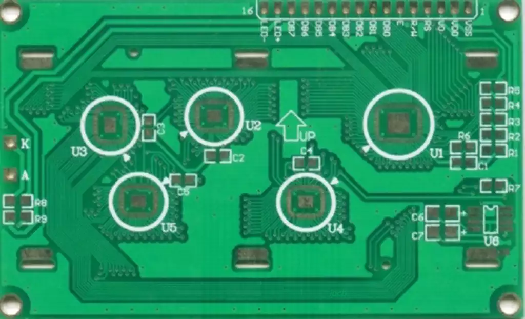
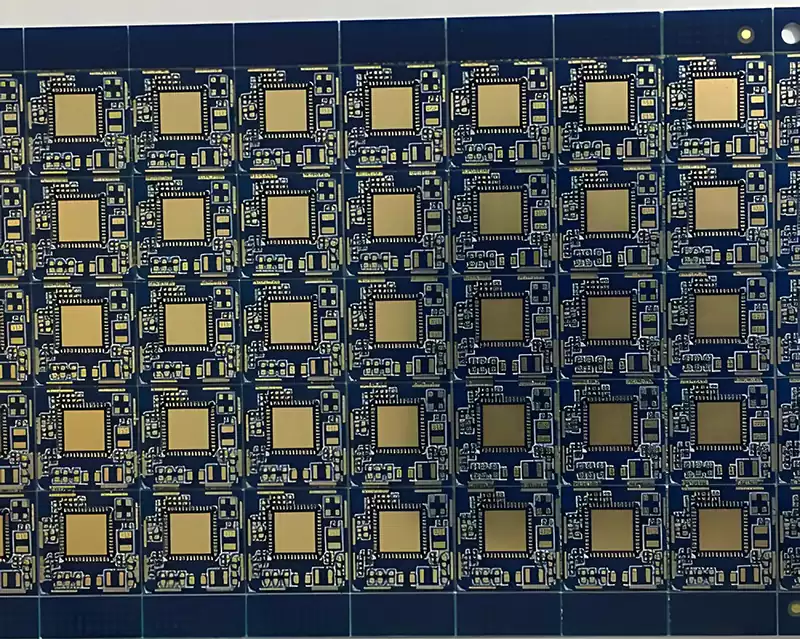
Introduction to the Characteristics of double sided pcb
The main difference between double-sided and single-sided boards lies in the number of copper layers: double sided pcbs have copper on both sides, with inter-layer connectivity achieved via plated-through holes; Single-sided boards have only one layer of copper and are limited to simple circuits; the holes are used solely for component insertion rather than electrical connectivity.
As routing density increases and hole diameters decrease, the quality of plated-through holes becomes critical to the reliability of double sided pcb. Small holes are prone to retaining debris such as grinding dust and volcanic ash, which can affect the chemical and electroplating processes, leading to defects where the holes are not properly plated.
Soldering Methods for double sided pcb
To ensure electrical conductivity in double-sided circuits, it is recommended to first solder the connecting holes on the double-sided board (i.e. the plated-through sections) using wires, then trim any sharp ends to prevent injury.
Soldering Guidelines:
Alignment: Align components according to the process drawings; align first, then insert.
Diodes: Place the component with the type designation facing upwards, ensuring both leads are of equal length.
Polarity: Polarised components must not be inserted upside down; integrated circuits, whether mounted vertically or horizontally, must not be noticeably tilted.
Soldering Iron Parameters: Power 25–40 W, tip temperature approximately 242°C, with single-point soldering time limited to 3–4 seconds. Excessive temperature may damage the soldering tip, whilst insufficient temperature will result in incomplete solder melting.
Soldering sequence: Proceed according to the principle of working from low to high and from the inside out. Avoid prolonged soldering to prevent scorching components or copper traces.
Processing frame: It is recommended to construct a processing frame to hold the circuit board, preventing pressure from tilting components that have already been soldered.
Final inspection: Conduct a comprehensive check for any missed components or unsoldered joints, trim excess leads, and then proceed to the next stage of the process.
Process Standards: Strictly adhere to relevant process standards to ensure soldering quality.
As electronic products evolve towards higher performance, miniaturisation and multifunctionality, double sided pcbs are widely used due to their higher routing density. Mastering soldering techniques and precautions can effectively improve the soldering quality and product reliability of double sided pcb.