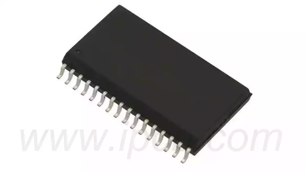
With the continuous advancement of communication technologies and the shift towards intelligent automotive electronics, market demand for high-power printed circuit boards and high frequency microwave pcbs continues to rise, becoming a key driver of growth in the printed circuit board industry. Microwave pcbs are manufactured using specialised microwave-grade copper-clad laminates in conjunction with conventional rigid board manufacturing processes, and are critical components for the proper functioning of high-frequency, high-speed electronic equipment. Their performance directly impacts signal transmission efficiency and equipment stability, and the choice of substrate is the fundamental factor determining the performance of microwave PCBs.
Currently, high-speed signal transmission is primarily divided into two application scenarios. One is high-frequency signal transmission, which utilises sine waves as the carrier and is widely used in fields such as radar detection, mobile communications, microwave communications and fibre-optic communications; the other is high-speed logic signal transmission, which utilises digital square-wave signals and was initially used in computers and servers, but has now expanded to various electronic products such as smart home devices and portable communication equipment.
The core requirements for both scenarios are low loss and low delay, which place stringent demands on the dielectric constant (Dk) and the tangent of the loss angle (Df) of the substrate material. Among the many substrate materials available, polytetrafluoroethylene (PTFE) has emerged as the optimal choice for high-frequency substrates due to its extremely low Dk and Df values, excellent resistance to high and low temperatures, and superior ageing resistance. It is also currently the most widely used substrate material in microwave pcbs.
The manufacture of microwave pcbs exhibits the following seven key specialisation characteristics:
1.Diversification of substrate selection, with a pronounced trend towards high-end products
In the early days, the domestic market relied heavily on domestically produced glass fibre-reinforced PTFE copper-clad laminates, but these suffered from issues such as limited variety and insufficient dielectric uniformity. Since the 1990s, products from the US-based Rogers Corporation, such as the RT/Duroid series, T series and RO4000 series, have entered the market, covering a variety of types including glass fibre-reinforced and ceramic-filled substrates. Although these are relatively expensive, they offer significant advantages in terms of dielectric stability and mechanical properties; in particular, Rogers substrates with aluminium backing have been widely adopted in high-end microwave equipment.
2.Refinement of Design Standards and Diversification of Functional Requirements
The manufacturing precision of microwave pcb patterns has gradually improved, whilst design complexity has increased. Board types have expanded from single- and double-sided boards to multilayer microwave pcbs; grounding design has placed higher demands on the metallisation of holes in PTFE substrates and the optimisation of grounding for aluminium-backed boards; plating processes have focused on enhancing the protection of aluminium substrates; and triple-proof protection—particularly for PTFE substrates—has also become a key design consideration.
3.Computerised production processes, enhancing both efficiency and precision
Traditional production relied on manual labour and was inefficient. With the widespread adoption of CAD/CAM/CAT systems, the manufacture of microwave printed circuit boards has achieved computerised control across the entire process—from high-precision stencil design and CNC machining to quality inspection—significantly improving production efficiency and product yield rates.
4.Specialisation in Pattern Fabrication, with Stricter Process Control
This involves technological upgrades across processes such as high-precision stencil fabrication, accurate pattern transfer and precision etching. Parameters must be optimised through process trials in accordance with product design requirements (e.g. whether holes are metallised and the type of surface coating), ensuring pattern accuracy meets the demands of signal transmission stability.
5.Diversification of Surface Coatings, Enhanced Protective Performance
The increasing complexity of application environments and the widespread use of aluminium substrate materials have set higher standards for plating and protection. Microstrip patterns generally employ nickel-gold electroplating to meet soldering requirements, whilst simultaneously requiring the development of triple-proof protection technologies that do not interfere with microwave signals. There is a growing demand for protection of aluminium substrates and for plating with metals such as silver and tin; this necessitates overcoming the bottlenecks in aluminium plating whilst safeguarding the microstrip patterns.
6.CNC-based contour machining to overcome mass production challenges
Particularly for microwave pcbs with aluminium substrates, traditional machining methods cannot simultaneously ensure precision, consistency and cycle times, making the adoption of advanced CNC technology essential. As the boards contain both metallic and non-metallic materials, the cutting tools, parameters and equipment required are highly specialised. Contour machining accounts for the largest proportion of the production cycle, directly impacting the progress of both R&D and mass production.
7.Automated batch inspection to ensure product consistency
In addition to standard continuity testing, microwave pcbs require inspection of characteristic impedance, pattern accuracy, positional accuracy, plating thickness and three-dimensional dimensional accuracy. Currently, the domestic industry largely relies on manual visual inspection, which is inefficient and prone to errors and omissions; the shift towards automated inspection is therefore an inevitable trend.
Basic requirements for high frequency microwave pcbs:
Precise matching of substrate parameters: Ensure that the dielectric constant, substrate thickness and copper foil thickness fully comply with design requirements.
Strict control of transmission line precision: Manufacturing precision is typically controlled within ±0.02 mm (±0.01 mm is also widely used), with edges that are smooth and free from burrs or notches.
Quality control of plating specifications: Particularly for plated-through-hole boards, plating thickness affects the total copper thickness and the precision of the conductors after etching; uniformity must be strictly controlled.
Machining accuracy compliance: Standard dimensional tolerances are ±0.1 mm; for high-precision products, these are ±0.05 mm or 0 to -0.1 mm, requiring specialised processes and equipment.
Core compliance with characteristic impedance: Characteristic impedance is the most fundamental and critical requirement and must be managed throughout the entire process.
During production, the following eight key stages must be closely monitored:
Precise handling of engineering data: Interpret the precision requirements for transmission lines and apply appropriate process compensation based on the factory’s manufacturing capabilities.
Scientific adaptation of cutting processes: Given the unique properties of microwave dielectric materials, milling and cutting should be the primary methods to avoid compromising flatness.
Precise control of drilling processes: Different dielectrics have varying requirements for drill bit point angle, cutting edge length and helix angle; aluminium-based and copper-based materials require special treatment to prevent burrs.
Proper grounding of through-holes: Plasma plating is recommended; as conventional copper plating is difficult on aluminium-based materials, it is advised to fill the holes with conductive metal material to ensure hole resistance ≤ 20Ω.
Precise and efficient pattern transfer: Select photoresist materials (photoresist, wet film, dry film) and corresponding exposure light sources that meet precision requirements.
Strict control of etching processes: Precisely control the composition, temperature and speed of the etching solution to ensure that conductor edges are flat and defect-free, and that precision standards are met.
Compliance with plating process specifications: Terminal coatings include tin-lead, tin-indium, silver and gold; pure gold plating is the most common application and must meet both soldering and protective requirements.
Optimisation of forming processes: CNC milling is the primary method, with significant variations in milling techniques across different materials; metal substrates require cooling with a neutral coolant, and milling parameters must be optimised.
Rogers PCB materials (such as the RO4000 and RT/Duroid series) are PTFE-based, offering stable dielectric properties and extremely low loss, perfectly meeting the core requirements of high-end microwave pcb for low loss and high reliability. Aimed at cutting-edge fields such as 6G, satellite internet and autonomous driving communications, microwave printed circuit boards are continuously evolving towards higher precision, greater reliability, miniaturisation and integration.