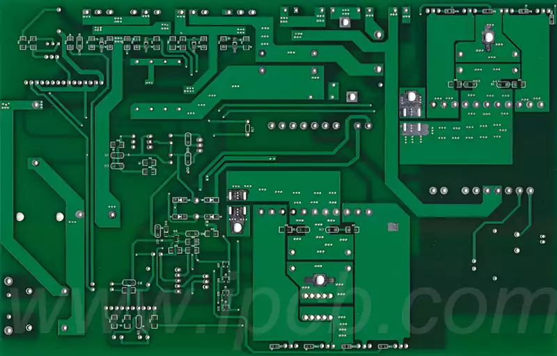
As the functionality of electronic products continues to evolve, the number of components mounted on PCBs is constantly increasing, component pin pitches are becoming increasingly fine, and circuit design is gradually shifting from conventional wide-pitch surface-mount technology to ultra-fine-pitch BGA layouts. Thanks to their high-density integration, excellent electrical performance and thermal management advantages, BGA (Ball Grid Array) packages have now become the mainstream packaging form for high-end controllers and chip-level devices.
However, this packaging presents extreme challenges in PCB layout, routing and via planning, and is a key bottleneck constraining production yield, signal quality and operational reliability. To balance electrical performance, power supply stability, manufacturing process compatibility and long-term operational reliability, it is essential to adhere to standardised BGA area routing and via design specifications. The specific design guidelines are as follows:
Core Design Specifications for BGA Area Vias
1.Via Selection Criteria
Micro blind and buried vias are preferred for high-density BGAs.
For precision-pitch BGAs with a pin-to-pin centre-to-centre distance of ≤0.8 mm, laser drilling processes should be prioritised for creating blind and buried vias, as this is the core solution for achieving efficient routing in confined spaces.
Mechanical Through-Holes for Standard Pitch
For BGAs with a pin pitch greater than 1.0 mm, low-density routing scenarios, or cost-controlled projects, traditional mechanical through-hole designs may be used. During the design phase, the space occupied by pads and reverse pads must be calculated in advance to avoid encroaching on routing channels.
Ultra-High Density: In-Pad Via Process
Placing laser-drilled micro blind vias directly at the centre of BGA pads represents the routing solution with the highest space utilisation currently available. This structure must be accompanied by resin via filling and electroplating to ensure a flat pad surface, thereby eliminating defects such as solder voids and cold solder joints at source.
2.Standardised via dimension design
All via diameters and pad sizes must strictly adhere to the PCB manufacturer’s process parameters. While meeting current-carrying and interlayer connectivity requirements, the smallest possible dimensions should be selected to free up more routing space.
Laser blind vias: Standard drilling diameter 4 mil, outer layer pad diameter 10 mil;
Mechanically drilled through-holes: Minimum drill diameter not less than 0.2 mm; outer layer pad with a single-side margin of ≥0.15 mm; industry-standard specifications include 8/18 mil and 10/20 mil;
During the early design phase, it is essential to liaise with the board manufacturer to confirm critical process parameters such as minimum drill diameter, minimum copper ring size and minimum hole spacing; designs exceeding these process limits are strictly prohibited.
3.Design of Via Pads and Ground Layer Isolation
Control the dimensions of via copper rings to ensure the copper width around the drill hole meets specifications, thereby enhancing the structural stability of the via walls. Power and ground layers must provide sufficient isolation rings for vias; the industry-standard minimum isolation distance is ≥0.15mm, effectively mitigating the risk of interlayer short circuits.
4.Via Spacing Control
Strictly distinguish between two types of spacing standards: the spacing between vias must adhere to the board manufacturer’s minimum process limit, typically not less than 0.2 mm; the spacing between the via body and signal lines or component pads must simultaneously meet electrical insulation requirements and manufacturing specifications, with dimensional tolerances precisely controlled in high-density areas.
5.Via Filling and Surface Treatment
Through-holes must be filled; the two main processes are resin insulation plugging and electroplated copper filling.
Resin plugging offers good value for money and is suitable for standard signal pins; electroplated filling provides superior thermal and electrical conductivity and is preferred for high-power heat dissipation pins and high-current pins.
Following via filling, a copper cap is electroplated to ensure the pads are smooth and level, preventing soldering defects caused by flux residue or solder paste accumulation;
Standard non-through-hole designs do not require via filling; for wave soldering applications, selective via filling may be performed as required to prevent molten solder from seeping into the holes.
6.BGA Pin Fan-Out Design
The core function of fan-out design is to smoothly route signals from the dense BGA pins to the outer layer routing channels. In practice, four key principles are followed:
Fan-out traces should be kept short and straight to minimise signal transmission paths;
The dogbone-style fan-out structure is the mainstream approach, where BGA pads are connected to fan-out vias via short leads; non-customised through-holes must not be placed directly adjacent to BGA pads;
Fan-out vias should be prioritised within the gaps between BGA pins; outer-layer pins may be routed with a moderate outward offset, whilst inner-layer high-density pins should primarily utilise through-hole vias;
Fan-out routing directions should be consistent and uniform, maintaining a consistent routing pattern for BGA arrays of the same specification to maximise the utilisation of on-board routing space.
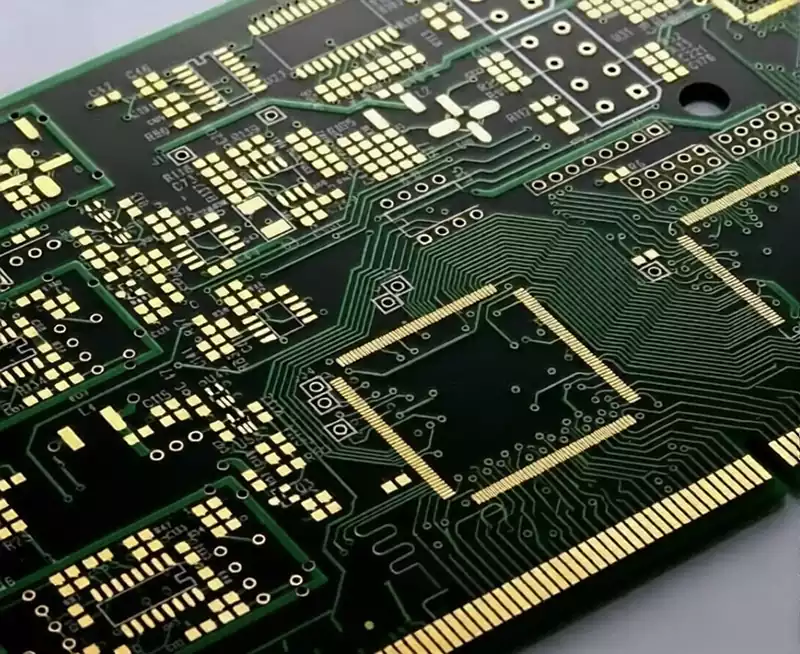
BGA Area Routing Design Specifications
Precise Matching of Line Width and Spacing to Process Requirements
Whilst ensuring compliance with impedance matching and current-carrying standards, fine line widths and spacings are selected to expand routing channels. Common specifications for high-density BGAs include 3/3mil, 3/4mil and 4/4mil; all line parameters must be confirmed in advance with the board manufacturer regarding their mass production capabilities.
Dimension Control for Tracing Within Pin Spacing
When routing inner-layer traces within BGA pad spacing, the trace width should be maintained at 4 mil or greater wherever possible, with a minimum safety spacing of 3.5 mil between traces. Excessively small dimensions significantly increase the likelihood of etching defects during production and limit the range of PCB manufacturers available for selection.
General DFM Principles for BGA Design
Prioritise alignment with upstream and downstream process capabilities
During the early design phase, liaise with the PCB manufacturer and SMT assembly plant to fully confirm core standards such as minimum line width and spacing, extreme drilling parameters, alignment accuracy, board material, and laminate process. All design solutions must be based on actual mass production processes.
Rational Planning of PCB Layer Stacks
Scientifically partition signal, power and ground planes to ensure sufficient routing layers for all pin connections whilst achieving uniform copper distribution across power and ground planes. Concurrently implement impedance control for high-speed signal lines and precisely manage interlayer dielectric thickness.
Detailed Optimisation to Improve Mass Production Yield
Incorporate teardrop designs: reinforce the connection points between traces and pads to enhance the mechanical resistance of the circuit to bending;
Standardise silkscreen layout: Position silkscreen characters away from BGA pads and via areas, clearly marking component orientation and the first pin identifier;
Optimise solder mask design: Ensure stable formation of solder mask bridges between pins; make solder mask openings 0.05–0.1 mm wider on each side than the solid pad;
Reserve test points: Strategically place functional test points in positions that facilitate probe contact, meeting the requirements for subsequent assembly testing.
PCB layout and routing for BGA packages constitute a systematic design process that must balance high-speed signal integrity, high-current power supply stability and chip thermal management requirements, whilst fully aligning with mass production manufacturing processes. The core design philosophy can be summarised in four points:
For ultra-fine-pitch, high-density BGAs, prioritise the implementation of laser-drilled blind and buried vias combined with in-pad via filling;
Strictly control all structural dimensions within the manufacturer’s process limits, minimising via diameters and optimising trace specifications;
Coordinate the board layer structure and pin fan-out methods to make efficient use of limited routing space;
Integrate DFM (Design for Manufacturability) principles throughout the entire process, balancing manufacturing convenience with long-term product reliability.
The key to BGA PCB design lies in achieving a balance between high-density interconnections, signal integrity, power stability and manufacturability within a limited space. Only by addressing high-density interconnections, signal integrity and manufacturability in the design can a BGA PCB with stable performance and leading yield rates be created.