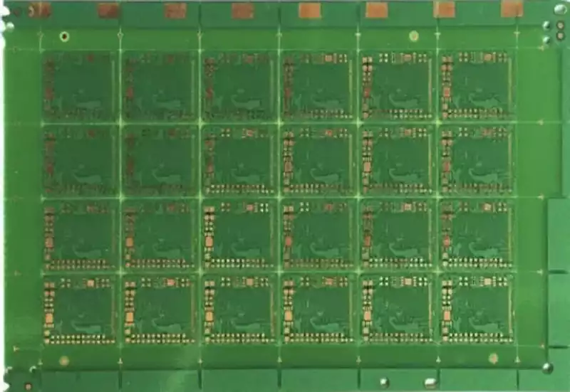
As a core foundational material in the high-end chip packaging process, the classification of IC substrates essentially follows a tiered matching principle of ‘material properties → structural form → application requirements’. Different types of IC substrates exhibit significant differences in key aspects such as wiring density, temperature resistance and production costs; these differences directly determine their scope and limitations of application across various high-end electronic sectors, and serve as the core basis for selecting chip packaging solutions.
Classification of IC Substrates
Classification by Material
1.BT Resin Substrates (Bismaleimide Triazine)
Performance Characteristics:
Outstanding high-temperature resistance, with a glass transition temperature (Tg) of ≥200°C and good dimensional stability. Possesses high rigidity and stable dielectric properties (Dk ≈ 4.0–4.5, Df ≈ 0.008–0.015). Medium routing density, with line widths/spacing typically ranging from 30 to 50 μm, capable of meeting the requirements of most mid-to-high-end packaging applications.
Advantages and Limitations:
Moderate cost, mature manufacturing processes, and good compatibility with various packaging formats such as BGA and CSP. The main limitation lies in its inability to support ultra-high-density routing (<20 μm), making it difficult to meet the demands of top-tier CPUs/GPUs for extreme interconnect density.
Typical Applications:
Mobile phone RF transceivers, automotive-grade MCUs (e.g. NXP S32K, Renesas RH850), mid-to-low-end application processors, DDR memory chips, etc. BT substrates are the most widely used and highest-volume substrate type in the mid-to-high-end electronics sector.
2.ABF Substrates (Ajinomoto Build-up Film)
Performance Characteristics:
Ultra-high wiring density is its defining feature. By using ABF film as the stacked dielectric layer, line widths and line spacings as low as 10–20 μm can be achieved (with advanced processes reaching 5–8 μm). It offers excellent surface flatness and superior interlayer insulation, making it perfectly compatible with C4 copper pillars or micro-bump arrays.
Advantages and Limitations:
Its performance sits at the very pinnacle of the industry, making it the material of choice for high-end computing chips requiring high-density, multi-pin packaging. However, production costs are extremely high and the manufacturing process is complex (requiring multiple layering, laser drilling and pulse electroplating). Production capacity is highly concentrated among a small number of companies, such as Ajinomoto, Unimicron, Samsung Electro-Mechanics and Nanya, resulting in limited supply flexibility.
Typical Applications:
Server CPUs (Intel Xeon, AMD EPYC), AI training/inference GPUs (NVIDIA H100/B200, AMD MI300X), FPGAs (Xilinx Versal), and high-end mobile SoCs (Apple A17 Pro, Qualcomm Snapdragon 8 Gen 3). The production capacity and technical standards of ABF substrates directly impact the global shipment capacity of high-end computing chips.
3.Epoxy-based Substrates (e.g. FR-4, FR-5)
Performance Characteristics:
Cost-effectiveness is the core advantage. Utilising traditional epoxy-glass fabric substrates, the manufacturing process is highly mature and material costs are low. The wiring density is relatively low (line width/spacing ≥50μm), temperature resistance is moderate (Tg ≈ 150–180°C), and dielectric loss is relatively high.
Advantages and limitations:
Their cost advantage is unrivalled, making them suitable for consumer-grade applications with modest performance requirements but high price sensitivity. They cannot meet stringent requirements such as high density, high temperature resistance, or low loss.
Typical Applications:
IoT sensors (temperature and humidity, motion, gas), Bluetooth/Wi-Fi chips, low-end MCUs (household appliances, toys, remote controls), and entry-level tablet/laptop controllers. In cost-driven scenarios, epoxy substrates hold an absolute dominant position.
4.Ceramic Substrates (Al₂O₃, AlN, BeO, etc.)
Performance Characteristics:
Exceptional thermal conductivity and high-temperature resistance are the unique advantages of ceramic substrates. Using aluminium oxide (Al₂O₃, thermal conductivity ≈20–30 W/m·K) or aluminium nitride (AlN, thermal conductivity ≈170–200 W/m·K) as the substrate material, their thermal conductivity is 10 to 100 times that of resin-based substrates. They can withstand temperatures exceeding 500°C whilst offering excellent insulation properties and radiation resistance.
Advantages and limitations:
Capable of withstanding extreme environments such as high temperatures, high power and intense radiation, their reliability far exceeds that of organic substrates. However, the materials are highly brittle, processing costs are high, and it is difficult to achieve thin, lightweight or flexible designs, resulting in relatively limited application scenarios.
Typical Applications:
Automotive power modules (IGBT, SiC MOSFET), aerospace electronics (satellite communications, attitude and orbit control), high-power LEDs, underground high-temperature sensors, and medical implantable devices (such as pacemakers requiring high-temperature sterilisation). Ceramic substrates are the ‘final safeguard in extreme environments’.
Classification by Structural Form
1.Rigid Substrates
Characteristics: The substrate is made of rigid materials (BT/epoxy + glass fibre cloth, or ceramic) and cannot be bent. It offers high structural strength and excellent resistance to vibration and impact.
Key Advantages: Outstanding structural support; highly compatible with mainstream packaging formats such as BGA, CSP and PGA; standardised manufacturing processes.
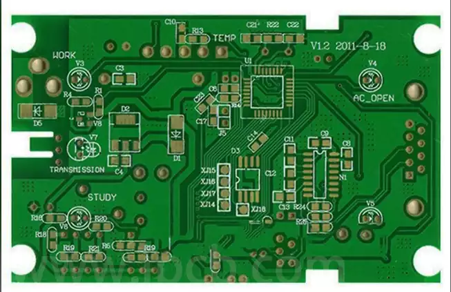
Market Position: Accounts for over 80% of the total IC substrate market share, covering most conventional devices such as servers, PCs, televisions, industrial control systems, base stations and general consumer electronics.
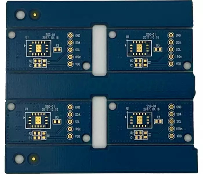
2.Flexible Substrates (FPC-based IC Substrates)
Physical Characteristics: Utilising polyimide (PI) or liquid crystal polymer (LCP) as the substrate, with thicknesses as thin as ≤0.1mm, these substrates are bendable, foldable and even rollable.
Key Advantages: Aligns with the trends towards slim, foldable and highly integrated consumer electronics, significantly saving internal space and enhancing design flexibility. High bend endurance (foldable smartphones can withstand hundreds of thousands of opening and closing cycles).
Typical Applications: Chips connecting the main and secondary boards at the hinge of foldable smartphones; main controllers for smartwatches and fitness trackers; SiP modules for TWS earphones; and bendable medical patches.
3.Rigid-Flex Substrates
Structural Features: Utilises an integrated composite structure comprising ‘rigid zones’ and ‘flexible zones’. The rigid zones provide support for chips and passive components, whilst the flexible zones enable three-dimensional routing to accommodate complex assembly paths.
Key Advantages: Combines the structural support of rigid materials with the routing flexibility of flexible materials, reducing the number of connectors and solder joints and enhancing overall system reliability.
Typical Applications: High-end automotive electronic modules (cockpit domain controllers, LiDAR control boards), portable medical diagnostic devices, endoscopes, and aerospace electronic equipment.
Classified by package type
Ball Grid Array (BGA) carrier boards: Designed for BGA packages, where the chip’s underside features a grid of solder balls as leads. This is the most common type of IC carrier board, used for the vast majority of mid- to high-end chips (CPUs, GPUs and ASICs).
Chip-Scale Package (CSP) Substrates: Designed for CSP packages, with substrate dimensions close to those of the chip itself (≤1.2 times). Primarily used for memory chips and RF front-end modules requiring extreme thinness and compactness.
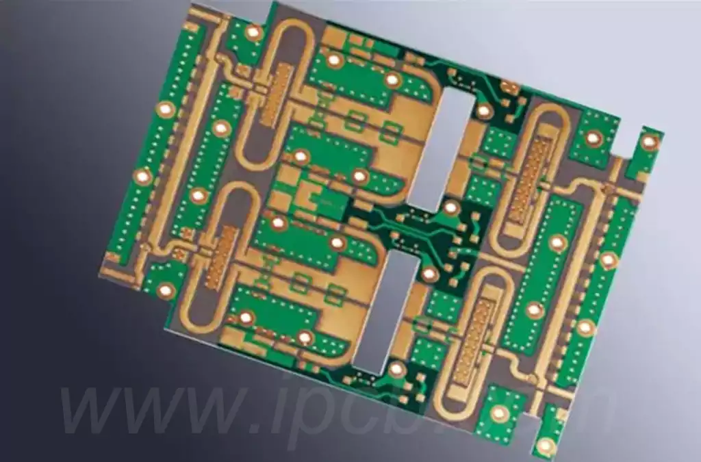
System-in-Package (SiP) Substrates: Support the integration of multiple bare chips (CPU, memory, power management, RF, etc.) into a single package. With extremely high routing complexity and density, these typically utilise high-end BT or ABF substrates, combined with embedded passive component technology.
With the development of 2.5D/3D advanced packaging, silicon interposers and hybrid bonding technologies are blurring the boundaries of traditional carrier boards; however, organic carrier boards still dominate in large-scale mass production.
Application Areas of IC Substrates
1.High-end computing (servers, AI, cloud computing)
Key requirements: ultra-high computing power, high-frequency signals, and a vast number of I/O pins (thousands). This necessitates extreme routing density to shorten signal paths and reduce losses; simultaneously, excellent thermal management and low dielectric loss (Df < 0.005) are required.
Suitable carrier boards: Almost exclusively ABF carrier boards (multi-layer, 12–20 layers); some ultra-large-scale AI chips utilise rigid-flex carrier boards for power management.
Specific Applications: AMD EPYC server CPUs, NVIDIA H100/B200 AI GPUs, Intel Xeon processors, and cloud-based FPGAs. The quality and supply of ABF carrier boards directly determine whether these chips can operate stably under power consumption of several hundred watts.
2.Consumer Electronics Sector (Mobile Phones, PCs, Wearables)
Core Requirements: Slim and lightweight design + high integration + tiered cost structures. Flagship models demand high density (SoC, RF), whilst mid-to-low-end models strictly control BOM costs.
Suitable Substrates:
High-end mobile SoCs (Apple A17, Snapdragon 8 Gen 4): ABF substrates (core areas) or high-end BT substrates;
RF/Bluetooth/Wi-Fi chips: BT substrates or low-cost epoxy substrates;
Foldable screens/wearable devices: Flexible substrates or rigid-flex substrates;
Entry-level consumer electronics: Epoxy resin substrates.
Cost logic: High-end ABF carrier boards account for 30%–50% of chip packaging costs, whilst low-end epoxy carrier boards account for only 10%–20%.
3.Automotive electronics sector (autonomous driving, domain controllers, power chips)
Key requirements: High reliability (compliant with AEC-Q100 Grade 0/1, operating temperature range -40°C to 150°C), vibration resistance, long service life (over 15 years). Power chips also require exceptional thermal conductivity.
Suitable Substrates:
Autonomous driving domain controllers (Mobileye EyeQ5/6, NVIDIA Orin), automotive-grade MCUs: Primarily BT resin substrates, balancing temperature resistance and reliability;
IGBTs and SiC power modules (inverters, OBCs): Ceramic substrates (AlN or Al₂O₃), utilising their high thermal conductivity to dissipate heat promptly;
In-vehicle infotainment systems: Some use epoxy or BT substrates.
Industry trends: The adoption of 800V high-voltage platforms and SiC is driving a surge in demand for ceramic substrates; smart cockpits and autonomous driving are driving an increase in the use of multi-layer HDI BT substrates.
4.Other High-End Applications
Internet of Things (IoT) and industrial control: Primarily utilises epoxy resin substrates (temperature and humidity sensors, industrial MCUs), with BT substrates selected for certain harsh environments (e.g. outdoor base stations).
Medical electronics: Rigid-flex substrates are used in portable diagnostic devices and endoscopes; ceramic substrates are selected for implantable devices (such as pacemakers) due to the requirements for high-temperature sterilisation and biocompatibility.
Aerospace: Satellites, missiles, spacecraft, etc., which face stringent requirements regarding temperature, radiation and vacuum, almost exclusively use ceramic substrates (AlN or BeO), with some paired with specialised BT substrates.
The selection of IC substrates can be summarised under the following three key considerations:
Performance Priorities
High-end chips (CPU/GPU/AI/FPGA) → ABF substrates (priority on wiring density)
Mid-to-high-end applications (automotive-grade/RF/storage) → BT substrates (balanced overall performance)
Cost-effective applications (IoT/entry-level consumer products) → Epoxy substrates (cost priority)
Extreme environments (high power/high temperature/radiation) → Ceramic substrates (thermal conductivity/temperature resistance priority)
Form Factor Compatibility
Foldable/ultra-thin/wearable devices → Flexible substrates or rigid-flex substrates
Conventional rigid devices (servers, industrial control, televisions) → Rigid substrates
Cost Logic
ABF and ceramic substrates belong to the high-end category, accounting for 30%–50% of the total packaging cost, and are primarily used for high-value individual chips.
BT substrates are a mid-range category, accounting for approximately 15%–30%.
Epoxy substrates are a low-end category, accounting for as little as 10% or less, and are suitable for high-volume, low-cost applications.
Future Technology Trends and Industry Outlook
ABF substrates are undergoing continuous upgrades: AI chips and HPC are driving the evolution of ABF towards 30 layers or more, with line widths/spacing of 5–10 μm.
Glass Core Substrates Emerge: Corning, Samsung Electro-Mechanics, Intel and others are developing glass-based IC substrates. Glass offers an ultra-low coefficient of thermal expansion (CTE close to that of silicon), higher flatness and superior electrical isolation properties. It is expected to replace some ABF and BT substrates in the future, being particularly suitable for 2.5D/3D integration and ultra-large-scale packaging.
Green Manufacturing and New Materials: Resins with low dielectric loss, halogen-free substrates and recyclable substrates are emerging as new directions driven by environmental considerations. Meanwhile, liquid crystal polymer (LCP) substrates for the millimetre-wave band are entering the commercialisation phase.
As the core foundational material for chip packaging, the characteristics of different IC substrates must be defined, and matched according to the three-dimensional balance of performance, form and cost; this is key to achieving the optimal packaging solution. As semiconductor processes evolve towards more advanced nodes, the importance of IC substrates will continue to grow.