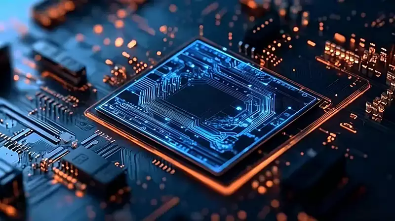
As the core component responsible for computing power transmission, signal exchange and power distribution within AI server PCB, high-layer-count, high-performance PCBs directly determine model training efficiency, system stability and data transmission limits. Among these, high-end PCBs featuring a 44-layer ultra-high-density architecture and utilising M9 ultra-low-loss speciality substrate have become the standard core hardware for the new generation of AI servers, completely revolutionising the design standards and materials systems of traditional servers.
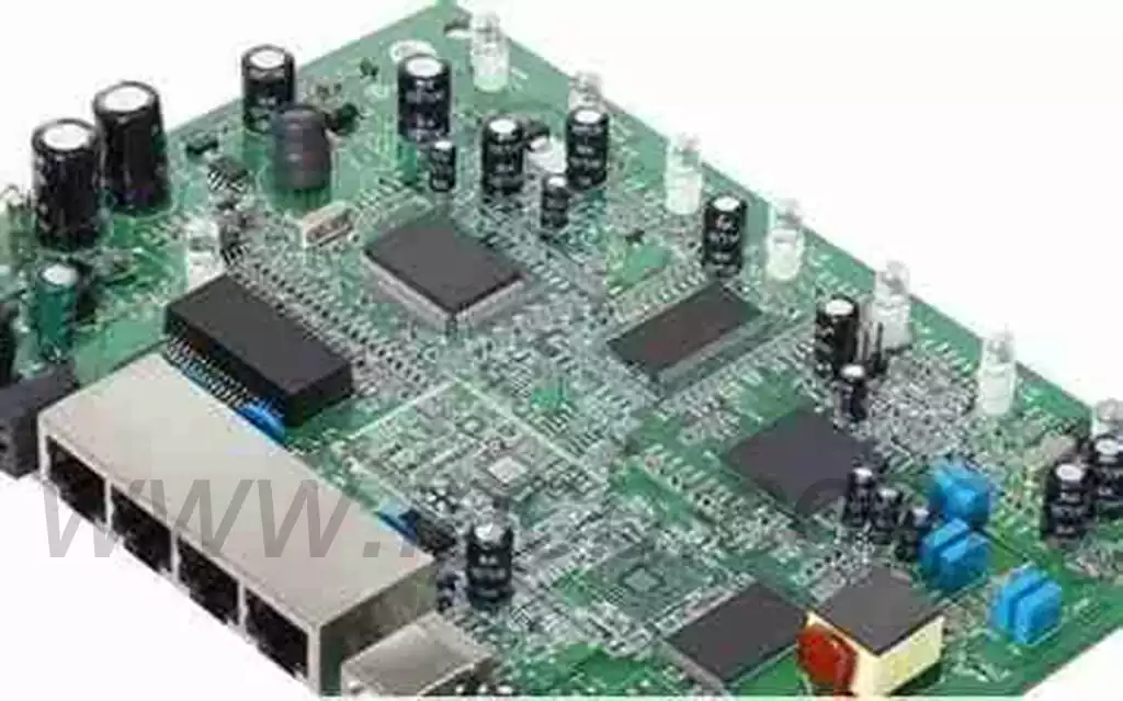
The hardware architecture of high-end AI server racks relies on five specialised PCB board types working in concert to build a comprehensive computing power transmission system: compute boards, switch boards, CPX boards, mid-plane boards and backplanes. Each performs its specific function whilst working in close coordination, forming the server’s internal ‘computing power skeleton and neural transmission network’, providing comprehensive support for massive data throughput, high-speed signal exchange and the continuous training of ultra-large parameter models.
Unlike standard consumer-grade or industrial-grade PCB boards, the material properties, layer stack design, manufacturing processes and thermal management capabilities of AI server PCBs directly determine the system’s signal integrity, transmission rates, thermal stability and long-term reliability. Consequently, the selection of substrate materials has become a key technological barrier for leading enterprises seeking to capture the high-end AI computing market.
Positioning and Material Selection for the Five Core PCB Boards
Computing Board: Responsible for the computational scheduling of core processing chips such as GPUs and TPUs, this is the core hardware for the parameter calculation and iteration of large models. As this board operates continuously under high load, generates significant heat and runs at high frequencies, it requires a balance between substrate stability, loss performance and cost.
Industry forecasts suggest that a standardised substrate solution will be formally established by the end of 2025, with a high probability of adopting the M8 ultra-low-loss material, which offers stable performance and better value for money, thereby effectively controlling the mass production costs of the entire system whilst meeting computing power requirements.
Switch Board: Responsible for high-speed data exchange and cross-card signal routing within the system, it serves as the central hub connecting all computing units, with extremely high demands on signal loss, transmission rates and impedance stability. With the widespread adoption of PCIe 5.0/6.0 and 400G/800G high-speed networks, the industry generally expects that, from late 2025 onwards, switch boards will be fully upgraded to M9 specialised materials to accommodate ultra-high-speed, high-capacity data exchange scenarios.
CPX Board: A dedicated computing acceleration board responsible for special algorithm acceleration, computing power optimisation and auxiliary computations. It alleviates the load on the core computing boards, thereby enhancing the overall efficiency of large-scale model training and inference. The industry has established clear selection criteria for its substrate material: the uniform adoption of ultra-low-loss materials of M9 grade or higher to completely eliminate high-frequency signal interference and transmission attenuation.
Backplane: The core interconnect within the AI server, linking the compute boards and CPX acceleration boards to establish high-speed data pathways throughout the system. As the board with the most complex architecture and the highest manufacturing difficulty in the current design, the middle board employs a 44-layer ultra-high-density laminate structure, far exceeding the layer count of traditional server PCBs.
Consequently, a top-tier material system is essential: centred on M9 ultra-low-loss substrate, paired with high-precision Q-step quartz cloth and fourth-generation high-purity copper foil, to meet the demands of ultra-long-distance, high-density, and high-speed signal transmission, whilst eliminating signal distortion and attenuation in complex link configurations.
Backplane: The fundamental support platform for the entire system, responsible for power distribution, basic signal transmission and the secure mounting of all boards. To accommodate the high-power, high-load characteristics of AI servers, the backplane is also specified to use high-end materials such as M9 or higher, establishing a robust hardware foundation to ensure stable power supply and reliable signal transmission.
The Core Logic Behind AI PCB Performance Upgrades
The evolution of PCB substrates for AI servers is not merely a matter of improving individual parameters, but rather a systematic upgrade centred on signal integrity, thermal management capabilities, long-term reliability and suitability for high-density manufacturing. As the mainstream materials for current high-end AI PCBs, M8 and M9 belong to the ultra-low-loss and extreme-low-loss categories respectively, exhibiting significant differences in performance levels and catering to different application scenarios for functional boards.
As a top-tier specialised substrate in the industry, M9’s core advantages lie in its extremely low dielectric loss and exceptionally high dielectric constant stability. In high-frequency, high-speed, long-distance, and multi-layer dense signal transmission scenarios, M9 minimises electromagnetic loss, suppressing signal attenuation, phase shift and waveform distortion, and is perfectly suited to ultra-complex stack-up structures such as 44-layer mid-plates.
Furthermore, M9 supports the formation of ultra-thick boards exceeding 3 mm in thickness, accommodates precision drilling processes with ultra-high thickness-to-diameter ratios of 15:1 or greater, and meets the manufacturing requirements for high-layer-count HDI boards ranging from 16 to 44 layers and beyond, making it an essential material for ultra-high-end AI server PCBs.
The performance of M8 is slightly inferior to that of M9—there are certain gaps in dielectric loss, thermal stability and process compatibility—but its mass production costs are lower, offering outstanding value for money. Consequently, M8 is better suited to scenarios such as compute boards, which serve as the core of computing power, are cost-sensitive and feature relatively regular signal transmission paths, ensuring stable computing output whilst balancing performance and cost.
As for switch boards, which require round-the-clock processing of high-speed data exchange across the entire network, a consensus has gradually emerged within the industry: the industry will fully transition to M9 materials to further enhance the system’s data exchange efficiency.
Design Challenges for High-Layer-Count High Speed PCBs
The core of high speed PCB design for AI servers lies in addressing three major challenges: signal distortion, electromagnetic crosstalk and thermal imbalance, all of which arise from high layer counts, high density and high frequencies. The requirements for stack-up layout, ground plane design and thermal management solutions are all more stringent than for traditional PCBs.
Signal Integrity Design: Core boards typically feature extremely high layer counts and substantial board thicknesses—switch boards commonly exceed 20 layers, with intermediate boards reaching up to 44 layers, and board thicknesses of ≥3mm. These are combined with ultra-fine 0.2mm via diameters and precision structures featuring an ultra-high aspect ratio of 15:1, placing extreme demands on impedance control accuracy.
Industry standards stipulate that impedance control tolerance for such high-end PCBs must be strictly maintained within ±5%, with even tighter tolerances required in high-precision applications to support next-generation high-speed protocols such as PCIe 5.0/6.0, DDR5, and 400G/800G Ethernet. To this end, high-layer-count PCBs move away from simple stacking, adopting a scientific architecture where signal layers, ground layers, signal layers and power layers are arranged alternately.
A low-impedance signal reference plane is constructed using a large, continuous copper-clad layer. All high-speed signal lines are routed internally and isolated by double-layer ground copper cladding, effectively shielding against external electromagnetic interference and resolving issues such as crosstalk, signal reflection and transmission distortion.
Thermal Management Design: AI servers generate high-density heat during prolonged, full-load training, and the limited internal space within high-layer-count PCBs makes heat accumulation highly likely. Consequently, high-end AI PCBs strictly require a substrate thermal conductivity of >3 W/m·K and a glass transition temperature (Tg) of >170°C, whilst also possessing an extremely low coefficient of thermal expansion (low CTE) to withstand high-temperature loads over the long term, thereby preventing deformation, warping or cracking.
For ultra-high-density boards such as 44-layer core boards, the industry generally adopts composite thermal management solutions: filling with thermal conductive media, designing high-density heat dissipation hole arrays, and optimising global heat dissipation paths; embedded copper blocks are introduced in high-power chip mounting areas to enhance heat dissipation; and the electroplating process is strictly controlled to ensure a plating thickness of ≥25μm that is uniform and consistent, thereby enhancing both electrical current-carrying capacity and thermal conductivity, and preventing equipment failure under high current and high temperature conditions.
The Technical Challenges of Precision Manufacturing for High-End AI PCBs
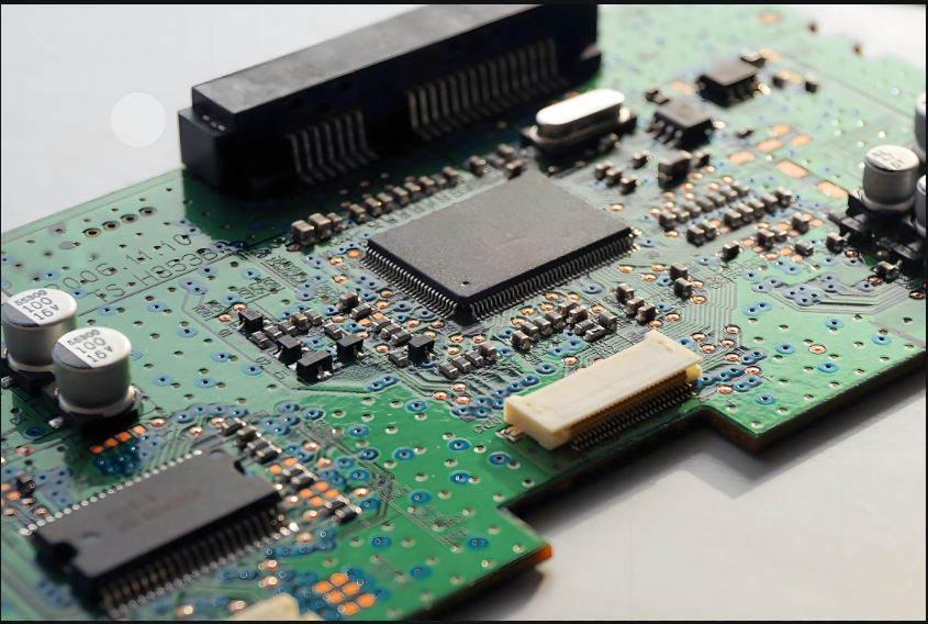
44-layer ultra-high-layer-count AI server PCBs represent the cutting edge of printed circuit board manufacturing today. The entire production process—including material forming, lamination, drilling, etching and inspection—involves extremely high technical barriers, making mass production impossible on standard production lines.
High-precision lamination and flatness control: The 44-layer composite structure is prone to issues such as uneven stress distribution and warping. This requires a precise layered lamination process and forming parameters tailored to M9 speciality materials to release internal stresses within the multilayer board and meet the requirements for high-precision surface-mount assembly.
Ultra-precision drilling and routing processes: To address the ultra-high aspect ratio of 15:1, laser micro-blind via processing technology is employed to precisely machine minute apertures, thereby reducing parasitic inductance at via locations and enhancing high-speed signal integrity. Concurrently, high-precision etching achieves ultra-fine line widths and spacings of 0.09 mm, maximising board space utilisation to meet the demands of massive signal transmission and routing.
Precise Impedance Testing and Simulation Optimisation: Prior to mass production, comprehensive testing is conducted using TDR automatic impedance testing equipment. Combined with SI signal integrity simulation tools, this enables comprehensive optimisation of the stack-up structure, routing layout and grounding design, correcting impedance deviations to ensure that every PCB is fully compatible with the operational requirements of high-speed AI computing.
PCB materials have become a key battleground in the competition for AI computing power
As the parameters of large AI models continue to break through from the trillion-level to the ten-trillion and hundred-trillion levels, and with the widespread adoption of 800G optical modules and next-generation high-speed protocols, the performance requirements for PCB materials in AI servers are constantly evolving, driving rapid iteration within the industry’s materials ecosystem. Compared to the telecommunications sector (where PCBs for 5G core networks and high-end switches have upgraded from 24 layers to 32 layers or more), the number of layers and the pace of material iteration in AI server PCBs are accelerating, making them the primary driver of PCB technology upgrades.
Overall, AI PCB materials are continuously evolving from ‘ultra-low loss’ towards ‘extreme low loss’. The current mainstream M9 still has room for improvement; in the future, a new generation of specialised substrates with superior performance will emerge, further reducing dielectric loss and enhancing thermal stability and process compatibility. The end of 2025 will mark a critical turning point—by then, material selection schemes for computing and switching boards will be formally implemented, which is highly likely to establish M9 as the mainstream standard for AI server PCBs, achieving full coverage of high-end materials across the five core board types.
Over the next five years, competition in AI computing infrastructure will shift entirely from superficial computing power stacking to core competition in underlying materials, hardware architecture and process technologies. AI server PCBs, once overshadowed by the GPU, have now become a key factor determining the energy efficiency, upper limits of computing power and system stability of AI computing centres. Continuous innovation and upgrading of PCB materials will serve as the cornerstone supporting the iteration of large models and the rapid development of the computing power industry, shaping the future technological landscape and market trends of high-end AI hardware.