The PCBA manufacturing process encompasses several core stages, including substrate pre-treatment, solder paste printing, component placement, reflow soldering, through-hole insertion, wave soldering, functional testing and final product inspection.The appropriate production processes vary significantly depending on the specifications and structure of the PCB;manufacturers select the appropriate manufacturing processes based on the PCB design, component types and mass production requirements to ensure the quality of the solder joints and the product’s performance.
Six Core Types of PCBA Manufacturing Processes
1.Single-sided SMT Assembly Process
This process involves single-sided surface-mount assembly, featuring a streamlined and efficient workflow. First, solder paste is precisely applied to the component pads on the bare PCB using a printing machine. Once the solder paste printing is complete, a fully automatic placement machine precisely positions various surface-mount components onto their corresponding pads. Finally, the board is fed into a reflow oven, where controlled heating melts and solidifies the solder paste, achieving both electrical connection and mechanical fixation of the components to the PCB. This is currently the standard process for lightweight circuit boards.
2.Single-sided DIP insertion process
This process addresses the single-sided processing requirements for through-hole components, with manual insertion forming the core of the operation. Production line operators insert various through-hole components, such as capacitors, sockets and switches, into pre-drilled holes on the PCB in accordance with process specifications.
Once insertion is complete, the PCB undergoes wave soldering to secure the components. Subsequently, excess leads are trimmed using a lead trimming machine, followed by a board cleaning process to remove flux residues and impurities from the board surface, thereby completing the basic manufacturing process. This process is suitable for traditional through-hole component PCBs; however, due to limitations in equipment and operational methods, overall mass production efficiency is relatively low.
3.Single-Sided Mixed Assembly Process
Single-sided mixed assembly combines both SMT (Surface Mount Technology) and DIP (Dual In-Line Package) insertion processing methods, and is suitable for PCBs that carry both surface-mount and through-hole components on a single side. During processing, SMT processes—such as solder paste printing, component placement, reflow soldering, and preliminary quality inspection—are completed first. Once it has been confirmed that the placement stage is free of misalignment, cold solder joints, or missed solder joints, the DIP insertion of through-hole components is then carried out.
The subsequent soldering method can be flexibly selected based on the number of through-hole components: if there are few through-hole components on the board, manual soldering is preferred to reduce equipment costs and process wastage; if there are a large number of components, wave soldering is used for batch production to improve production efficiency.
4.Single-sided SMT + DIP Dual-sided Hybrid Process
This process is primarily applied to double-sided PCBs, employing distinct processing methods on each side: one side undergoes SMT assembly, whilst the other undergoes DIP insertion. The basic operational procedures for single-sided SMT and single-sided DIP are identical to those of conventional single-sided SMT and single-sided DIP processes.
The distinction lies in the fact that when double-sided boards undergo processing via reflow or wave soldering equipment, specialised positioning jigs must be used to secure and protect the board. This prevents damage to the board surface, component displacement and solder bridging, thereby ensuring the precision and quality of the double-sided processing.
5.Double-Sided SMT Assembly Process
To optimise PCB board space utilisation, reduce board dimensions and enhance circuit integration, most precision circuit boards employ a double-sided SMT assembly process. The process design adheres to the principle of functional zoning, typically placing larger, pin-dense IC core components on the A-side of the PCB, whilst mounting compact surface-mount resistors, capacitors and other micro-components on the B-side. By utilising the board space comprehensively on both sides, the volume of the PCB is minimised whilst ensuring complete circuit functionality and a neat product appearance. This is widely used in miniaturised products such as precision electronics and smart devices.
6.Double-sided mixed assembly process
The dual-sided mixed assembly process is suited to complex PCBs where both surface-mount and through-hole components are present on both sides. Within the industry, there are primarily two processing approaches, each with distinct advantages, disadvantages and suitable application scenarios. The first is the three-stage heating assembly method, which requires the entire process to undergo three high-temperature heating cycles. This results in low production efficiency, and the accompanying hot melt adhesive process yields a low soldering pass rate during wave soldering, leading to insufficient quality stability; as such, it is generally not recommended at present.
The second is the differentiated soldering approach, which can be flexibly adjusted according to the component ratio on the board: when there are many surface-mount components and very few through-hole (THT) components, manual soldering can meet production requirements and offers better value for money; when there are a large number of THT components and high-volume production is required, wave soldering is the preferred method, balancing efficiency and soldering quality.
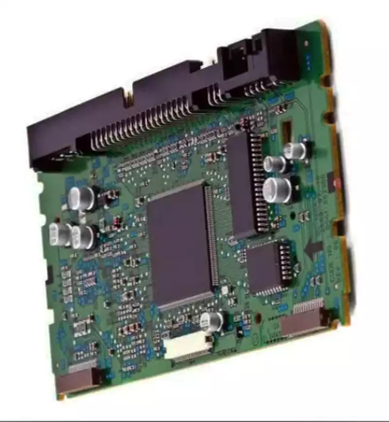
Key Steps in PCBA Manufacturing
1.Solder Paste Printing
As the first key process in PCBA manufacturing, this directly determines the quality of subsequent soldering. During operation, the equipment’s squeegee moves at a constant speed in close contact with the surface of the stencil, causing the solder paste to move smoothly. When the solder paste covers the apertures in the stencil, the vertical downward pressure exerted by the squeegee pushes the paste precisely through the apertures, depositing it evenly onto the corresponding component pads on the PCB. This provides the necessary solder support for subsequent component soldering.
2.Adhesive Application (Optional Process)
This process is applicable only to double-sided PCBs and serves as a preventative auxiliary step. During the manufacturing of double-sided PCBs, components mounted on the underside are prone to melting, detaching, or shifting during the high-temperature stages of secondary reflow soldering or wave soldering. By applying a specialised adhesive to the junction between the component’s underside and the board surface, the component’s position is secured in advance, effectively preventing component detachment caused by high-temperature processing and ensuring the stability of double-sided manufacturing.
3.Component Placement
This process is carried out using fully automated placement machines. The equipment utilises a precise positioning system to automatically pick up various surface-mount components from the component feeders. By aligning with the PCB’s positioning reference points, the components are placed with high precision onto the pads coated with solder paste. This ensures accurate component placement and a flat, even fit, eliminating issues such as misalignment, skewing, or missed placements. It is a core process in automated mass production.
4.Pre- and Post-Soldering Quality Inspection
Prior to soldering, a comprehensive inspection of the assembled circuit board is required, focusing on component placement, orientation and contact. Any defects such as misalignment, incorrect placement, omissions or tombstoning are promptly corrected to prevent soldering defects at source. Following soldering, the board’s solder joints are re-inspected to identify common defects such as cold solder joints, false solder joints, solder bridges or insufficient solder, thereby safeguarding quality for subsequent processes.
5.Reflow Soldering
Once component placement and pre-soldering inspections are complete, the circuit boards are fed into the reflow soldering equipment. Using a temperature-controlled hot-air convection process, the boards are heated gradually according to a preset temperature profile. This ensures the solder paste on the pads is fully melted and wetted. Upon cooling and solidification, this process simultaneously achieves mechanical fixation and electrical continuity between the component leads and the PCB pads, forming a stable and reliable solder joint.
6.Component Insertion
This process is primarily used for various through-hole components, as well as certain special surface-mount components that cannot be accommodated by placement machines, including through-hole electrolytic capacitors, connectors, push-button switches, and metal-lead-frame (MELF) components. Depending on component specifications and mass production requirements, either manual precision insertion or batch processing using fully automated insertion equipment can be selected to ensure secure component mounting and accurate hole alignment.
7.Wave Soldering
This process is the core soldering technique for through-hole components. Equipment is used to form a steady wave of molten solder, through which the assembled PCB passes at a constant speed. This allows the solder to fully wet the component leads and PCB holes, rapidly completing batch soldering and fixing, and is suitable for large-scale soldering operations involving various through-hole components.
8.Board Cleaning
After soldering, the surface of the circuit board is left with residues such as flux, solder dross, dust and oil. Specialised cleaning equipment and detergents are used to thoroughly clean the board surface, removing all types of residual contaminants. This prevents long-term adhesion of impurities that could lead to board corrosion, poor insulation or short circuits, thereby enhancing the product’s service life and stability.
9.Product Repair
This constitutes an auxiliary repair process outside the production line, carrying out targeted repairs on defective products identified during quality inspection. Key tasks include rectifying defective solder joints, re-soldering areas with cold or missed solder joints, and replacing damaged or failed components. This enables the cost-effective and efficient repair of defective products without compromising performance, thereby reducing production wastage and scrap costs.
10.Electrical Performance Testing
This process is used to verify the electrical continuity and functional integrity of PCB boards. It comprises two core testing modules: firstly, in-line testing, which focuses on detecting basic electrical issues such as circuit continuity, component parameters, short circuits and open circuits; and secondly, functional testing, which simulates actual operating conditions to verify whether the board’s overall functionality meets design standards and to identify products with functional defects.
11.End-to-End Quality Control
This process spans the entire production cycle and is divided into two main areas: in-process quality control and final product quality assurance. In-process quality control focuses on every stage of the production line, monitoring the quality of operations in real time across all stages—including printing, assembly, soldering and cleaning—and promptly identifying and rectifying any production anomalies. Final product quality assurance involves standardised verification of completed products, strictly controlling the quality of finished goods to ensure that products leaving the factory comply with industry and customer standards.
12.Finished Product Packaging and Post-Packaging Inspection
Once all production and quality inspection procedures have been completed, qualified PCBA products are packaged in accordance with standardised procedures to prevent issues such as impact damage, moisture ingress or contamination during transport and storage. Concurrently, post-packaging inspections are conducted in accordance with industry sampling standards, involving random checks of product performance and appearance. This provides a secondary layer of quality control to ensure that products delivered to customers consistently meet the required standards.