The Paradoxical Unity of Light and Electricity: Deciphering the Physical Essence of ITO Glass Substrates
In the world of materials science, “conductivity” and “transparency” are often seen as mutually exclusive enemies.
According to the fundamental laws of solid-state physics, metals like copper, aluminum, and gold have excellent electrical conductivity because they are filled with a dense array of freely moving “free electrons.” However, it is precisely these excessively dense free electrons that strongly reflect and absorb incoming visible light, causing the metals to appear opaque with a metallic luster.
Conversely, insulators like ordinary window glass, quartz, and plastics, because their internal electrons are tightly bound and unable to move freely, allow light to pass through easily; they are transparent but completely non-conductive. To break this curse of physical laws, scientists have developed a special class of disruptive materials—transparent conductive oxides (TCOs)—through extremely sophisticated chemical doping. The most successful commercialization story is that of indium tin oxide (ITO), obtained by microscopically mixing indium oxide (IN2O3) and tin oxide (SNO2) in a specific ratio (usually 90:10).
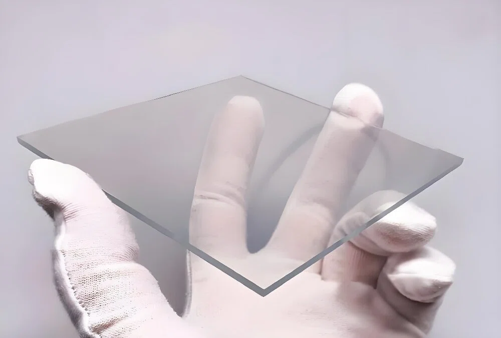
When we uniformly “bombard” a thin film of ITO, only tens to two hundred nanometers in size (equivalent to a few thousandths of the diameter of a human hair), onto an ultra-precision polished glass surface using high-vacuum magnetron sputtering technology, we create the cornerstone material of the optoelectronics industry: ITO glass substrate.
The magic of microscopic mixing: How does it achieve both transparency and conductivity?
We can figuratively compare the ITO glass substrate to a “molecular-level high-speed iron sunshade.” In the crystal lattice microstructure, indium oxide itself is an insulating ceramic network. However, when high-valence tin atoms forcefully squeeze into the indium oxide lattice, replacing some of the indium atoms’ positions, because the tin atoms have more electrons in their outer shells, they release a large number of “free carriers” (electrons) inside the lattice. It is these forcibly released electrons that endow the thin film, originally an insulating ceramic, with extremely excellent electrical conductivity, making it exhibit conductivity properties similar to N-type semiconductors.
So how does it remain transparent? This depends on the extreme thinness of the conductive layer and its wide bandgap. ITO material has a very wide energy bandgap, meaning that the energy of visible light (wavelength 400nm to 700nm) is too low to be absorbed by the electrons inside ITO. Visible light walks on the street, and the electrons inside ITO simply watch it pass by without any interception, allowing light transmittance to easily exceed 85% or even 90%. Because it can conduct current like a metal and allow 100% light transmission like air, it has become an indispensable “transparent positive and negative electrode” in the manufacture of liquid crystal displays (LCDs), organic light-emitting diodes (OLEDs), capacitive touchscreens, and solar panels. Without it, our smartphone screens would be nothing more than a black plate of metal, unable to display images while simultaneously sensing touch gestures.
The Core Game in Industrial Procurement: Balancing Sheet Resistance and Thickness
In the supply chain and technical specifications of ITO glass substrates, the two most crucial indicators are sheet resistance (usually expressed in Ω/□ ohms/square) and transmittance.
In daily technical exchanges, many inexperienced procurement personnel often make an unrealistic perfectionist demand: “I need an ITO glass with extremely low resistance (extremely fast conduction) and a transmittance of over 95%.” At this point, experienced board manufacturers and supply chain experts will incisively point out that, in physics, low resistance and high transmittance are an irreconcilable seesaw.
If we want extremely low sheet resistance (e.g., below 10Ω/□) to allow for rapid current flow, we must increase the deposition thickness of the ITO film. However, as the film thickness increases, the number of electrons and metal oxide particles accumulated inside surges. These particles begin to aggressively intercept and scatter visible light, causing the film to yellow and darken, and the transmittance to drop drastically.
Conversely, if we make the film layer very thin for ultimate visual clarity, the sheet resistance will soar to 100Ω/□ or even higher due to the extremely sparse number of free electrons inside, causing severe delays and heat generation in signal transmission. Therefore, the art of a top-tier supply chain lies in “precise tuning” based on the specific application scenario of the customer: If the customer is making large-area capacitive touchscreens for high-end mobile phones, in pursuit of millisecond-level touch response speed, a slight sacrifice in brightness must be made, choosing a low-impedance substrate of 15 to 30Ω/□. If the customer is making laboratory biosensors, electrochemical chips, or miniature liquid crystal dimming valves, with extremely short signal transmission distances but extremely stringent requirements for light purity, then a high-transmittance, ultra-thin substrate of 80 to 100Ω/□ should be prioritized.
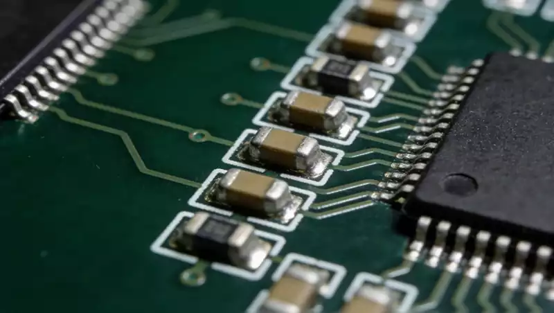
The Microscopic Sculpture Hell of Patterning: A Symphony of Strong Acid and Photolithography
After obtaining a large-area, fully conductive ITO glass substrate, it cannot be used directly. Because overall conductivity means it’s a single large electrode, soldering different signal pins onto it would instantly cause a massive short circuit. To enable it to transmit complex control signals, we must “carve” independent, non-interfering micron-sized transparent conductive lines and mesh structures onto the originally uniform and dense conductive film. This micro-processing that transforms “overall conductivity” into “local conductivity” is known in industry as patterning or etching.
Traditional Chemical Wet Etching: Dancing with Strong Acid on a Mirror
In mass production lines, chemical wet etching remains the most widely used technique. The entire process is very similar to the photolithography process for traditional semiconductor wafers. First, a layer of photoresist, a polymeric organic material extremely sensitive to specific wavelengths of light, is uniformly coated onto the conductive surface of the ITO glass. Second, a high-precision mask with a detailed circuit pattern is placed above it and precisely irradiated with intense ultraviolet (UV) light. After being bombarded by ultraviolet light, the molecular chains of the photoresist break down and are subsequently cleaned away in the developing solution. This effectively protects the area beneath the desired ITO pattern while exposing the unwanted ITO areas. The third step is the most nerve-wracking part of the entire process: a “strong acid baptism.”
Workers immerse the entire large glass block in a special aqua regia or acidic etching solution made from a high-concentration mixture of hydrochloric acid (HCl) and nitric acid (HNO3). As a metal oxide ceramic, ITO rapidly reacts chemically under the intense attack of the acid, transforming into soluble indium and tin salts, which are completely dissolved and washed away by the water flow within minutes. During this stage, process engineers must precisely control three variables: the temperature and concentration of the acid solution, and the immersion time. If the immersion time is too short (under-etching), the unwanted ITO areas will not be completely dissolved, leaving intermittent conductive burrs on a microscopic scale, causing fatal micro-short circuits between adjacent transparent traces. If the soaking time is even slightly longer, even by a few seconds (over-etching), the acid will not only dissolve vertically downwards but also “hollow out” the edges laterally, secretly eating away at the edges of the useful traces protected by the photoresist. This will lead to a significant reduction in the actual width of the traces, a sharp increase in impedance, and even microscopic open circuits. This process control of using strong acid to “dance” on a mirror surface only a few hundred nanometers thick is a core technological strength of PCB manufacturers.
Nanoscale Laser Dry Etching: Physical Evaporation Without Chemical Pollution
With the explosion of green manufacturing and ultra-high precision automotive instrument displays and wearable micro-displays (Micro-LEDs), traditional chemical pickling processes generate large amounts of heavy metal-laden acidic wastewater and, due to the capillary effect of liquids, cannot achieve the limit linewidth of less than 5 micrometers. To overcome this bottleneck, the industry has introduced laser dry etching. This process directly eliminates all photoresist and strong acid liquids. The PCB manufacturer uses an ultraviolet laser with extremely short wavelength and high energy density, employing a high-precision scanning mirror to directly scan the ITO thin film on the glass surface. When the laser is focused on a microscopic point, the instantaneous localized high temperature directly exceeds the melting and boiling points of the ITO ceramic, causing the metal oxide in the target area to undergo physical vapor evaporation (Ablation) within microseconds, directly vaporizing into gas and being vacuum-evaporated. The precision of laser dry etching is entirely controlled by optical and mechanical motors, resulting in clean, sharp edges like a knife cut, easily achieving micrometer-level linewidths, and zero wastewater discharge throughout the process. However, its core drawback lies in the extremely high depreciation cost of the equipment. Furthermore, even a slight drift in laser energy control can either fail to burn through the ITO or result in excessive energy creating microscopic “Great Rift Valleys” on the underlying glass substrate, causing localized stress concentration and easy breakage during subsequent assembly and handling.
Interface Impedance and Soldering Hell: How to Achieve a Perfect Bond Between Traditional Copper Conductors and ITO?
After successfully etching perfect transparent traces onto the ITO glass substrate, the next hellish problem arises: how to connect external ordinary control PCBs, flexible circuit boards (FFC/FPC), or driver chips to these transparent traces on the glass?
Here, we must emphasize a harsh fact of metal physics: traditional lead-free solder paste and soldering irons are completely ineffective on ITO surfaces. Ordinary tin/silver/copper (SAC) solder can firmly bond two copper wires together because molten tin undergoes atomic-level interdiffusion with copper, forming a strong intermetallic compound (IMC) layer at the interface. However, the physical nature of ITO film is a completely oxidized, dense ceramic layer. This is like trying to solder a ceramic bowl or glass window; molten tin dripping onto it will only form a round bead, which will fall off with a slight touch after solidification, failing to form any mechanical or electrical connection.
To break this deadlock in the connection between ceramic and metal, the electronics industry was forced to invent a revolutionary soldering process completely different from ordinary PCB assembly—Anisotropic Conductive Film (ACF) bonding.
The magic of ACF: A special “glue” that conducts only vertically and never horizontally. ACF technology requires no solder or high-temperature reflow ovens. Its core carrier is a special double-sided tape. Inside this tape, a high-molecular insulating epoxy resin (Glue) forms the matrix, with countless tiny conductive gold particles evenly suspended and encased within the resin. These conductive gold particles are typically only 3 to 5 micrometers in diameter, with an elastic plastic core and an outer layer of highly conductive nickel and gold.
The specific assembly process is as precise as magic: First, workers perform extremely precise optical alignment under a microscope between the copper-gold leads of the densely pinned flexible printed circuit board (FPC) and the ITO transparent leads on the glass substrate. The second step involves sandwiching a thin layer of ACF tape between the two. The third step uses an expensive cryogenic bonding machine (Pulse Bonder), employing a hot press head made of high-hardness diamond or titanium alloy to press firmly into the connection area, applying pressure of two to three hundred atmospheres and a temperature exceeding one hundred degrees Celsius.
Under this intense vertical mechanical pressure, the conductive gold balls sandwiched directly beneath the FPC copper leads and glass ITO leads are forcefully “flattened.” The gold layer on the outer surface of the gold balls is tightly pressed against the copper and ITO ceramic surfaces, thus creating conductive physical channels in the vertical direction. Meanwhile, in the gaps without leads, the conductive gold balls remain intact, suspended in the insulating resin, maintaining a safe distance between them, as they are not subjected to the vertical pressure of the hot press head. This adhesive layer remains an absolute insulator in the horizontal direction. This unique anisotropic physical property perfectly solves the conductivity problem of high-density transparent pins, achieving strong adhesion while ensuring that lateral short circuits between adjacent pins never occur.
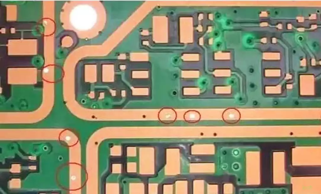
However, the invisible killer of contact resistance: While ACF solves the connection problem, because it relies on mechanical extrusion contact rather than the atomic-level melting welding of traditional solder, its contact resistance at the interface is several orders of magnitude higher than that of ordinary PCB soldering. If the pressure of the hot press head on the production line is slightly insufficient, or if the ITO film on the glass surface is left in the air for too long and a thick layer of microscopic organic contaminants adsorbs onto the surface (which physically changes the work function and interface potential of ITO), the conductive gold ball cannot completely pierce the contaminant layer to contact the ITO core. This causes the contact resistance to spike instantly. When the drive current passes through this tiny glue interface, the high resistance triggers intense localized Joule heating, causing the surrounding epoxy resin to age, crack, and peel off rapidly, ultimately resulting in large-area “dead lines” on the display or complete sensor signal failure.
To completely eliminate this invisible killer, modern ITO glass substrate bonding production lines must include a plasma surface cleaning process before ACF hot pressing. By bombarding the ITO surface with high-energy argon or oxygen plasma in a vacuum, organic oils and carbohydrates on the glass surface are completely blasted away and evaporated at the nanoscale using purely physical and microscopic chemical reactions, revealing an absolutely pure ITO crystal structure. This process is the absolute industrial trump card ensuring a 99.99% interface yield rate during mass production.
The “Invisible Backbone” of the Global Display, Energy, and Sensor Supply Chain
Having gained a deep understanding of the material nature of ITO glass substrate, its micro-patterning process, and ACF soldering, let’s step back and examine its true role in the entire electronics industry supply chain.
It’s not a rare sample in a laboratory, but an industrial behemoth producing hundreds of thousands of square meters daily. From upstream mining to downstream consumer goods, it forms the invisible backbone of the global display, green energy, and cutting-edge sensor supply chain.
At the very top of the supply chain: the key to manufacturing high-end ITO glass substrates lies in indium, a byproduct metal extremely scarce in the Earth’s crust. Indium is not formed independently; it is typically recovered with great difficulty as a byproduct trace element during the smelting of lead-zinc and copper mines. Global indium resources are extremely unevenly distributed, with China possessing the world’s largest share of indium reserves and production. In the actual operation of the supply chain, ITO thin films are made by bombarding and evaporating high-purity ITO targets onto the glass surface using magnetron sputtering. The purity of the target material must reach 99.99% (4N level) or even higher. Any excess iron, copper, or lead impurities mixed into the target material will form microscopic charge traps within the bombarded film, resulting in extremely uneven sheet resistance distribution across the entire glass substrate, or optically visible dark spots with color differences.
Therefore, upstream high-purity target material manufacturing technologies (such as target sintering density and isotropic crystal control) have long been controlled by Japan’s Mitsui and JX Metals, as well as a few top Chinese materials giants, forming an extremely solid material barrier.
Downstream Applications: The “Three Pillars” Downstream, ITO glass substrate firmly dominates three trillion-dollar super-sectors: Flat panel displays and touch panels (LCD/OLED/Touch Panels): This is the largest consumer market for ITO glass. Whether it’s televisions, computer monitors, in-vehicle central control screens, or smartwatches, the rotation control of liquid crystal molecules within them all requires ITO glass as a transparent electrode to provide a uniform longitudinal electric field. In touch panels, ITO is etched into orthogonal diamond-shaped or grid-like arrays, precisely locking coordinates through subtle capacitance changes triggered by finger touch.
Next-Generation Photovoltaics: In cutting-edge photovoltaic technologies such as heterojunction (HJT) solar cells and perovskite thin-film batteries, ITO glass plays a crucial role as the top transparent front electrode. It must allow unobstructed sunlight to penetrate and reach the underlying silicon wafer or perovskite light-absorbing layer to excite electrons, and simultaneously collect these delicate electrons and guide them into the external power grid. The balance between its conductivity and transmittance directly determines the power conversion efficiency of the entire photovoltaic power plant.
Smart Glass/Low-E Windows: Modern high-end building curtain walls and panoramic sunroofs of luxury cars increasingly utilize “electrochromic smart glass.” The inner sides of both layers of this glass are entirely covered with an ITO conductive layer. When a small voltage of a few volts is applied to the two layers of ITO, the electrochromic material sandwiched between them undergoes a redox reaction, instantly changing from completely transparent to a deep blue or black color, thus blocking glaring sunlight and infrared heat while maintaining privacy inside buildings and vehicles.