Microscopic Photochemical Film: Deciphering the Material Essence of Presensitized PCB board
In the era of modern electronics manufacturing, heavily reliant on large-scale automated factories, it’s hard for the average person to imagine that, without high-precision laser direct imaging (LDI) lithography machines, a high-precision PCB with linewidths accurate to a few mils could be manufactured in just ten minutes using only a simple ultraviolet lamp and a few containers of chemicals.
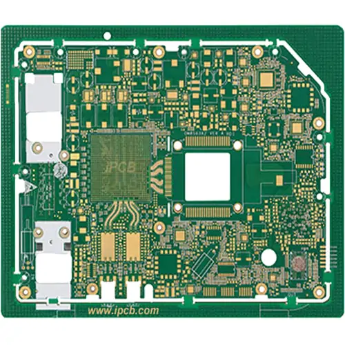
This miraculous material, enabling hardware engineers and laboratory researchers to achieve “self-sufficiency” in the prototyping stage, is called presensitized copper clad laminate, or presensitized PCB board in the international supply chain.
If we analyze it at a microscopic level, it is actually a highly complex “photochemical sandwich structure.”
The bottom layer is a common FR4 epoxy resin glass fiber substrate (substrate skeleton), and the middle layer is traditional ultra-thin, high-purity electrolytic copper foil (responsible for future electrical conduction). What truly gives it its “presensitized” essence is the top layer—a thin, high-molecular-weight organic chemical film, only a few micrometers thick, highly sensitive to specific wavelengths of ultraviolet light, applied uniformly in a cleanroom by the PCB manufacturer using a precision roller coating process. This film is either a presensitized dry film or a liquid photoresist.
The Physical Magic Beneath the Blue Protective Film: Photopolymerization and Photodegradation
We can understand this with a vivid analogy: a presented PCB board is essentially the color film of the electronics world.
When you first take it out of its vacuum-sealed packaging, you’ll see a semi-transparent, dark blue protective film covering its surface. This film blocks visible light and trace amounts of ultraviolet light from the environment, preventing premature chemical degradation of the photosensitive layer inside.
When engineers peel off this blue protective film and, in a darkroom or low-light environment, press a high-definition transparent film printed with complex circuit patterns tightly onto the board surface, then illuminate it with a regular ultraviolet (UV) lamp, the microscopic photochemical magic begins. Based on the different properties of the photosensitive adhesive layer material, there are two main physical approaches:
Positive Resist: This is the most mainstream type on the market and the most favored by engineers. Under the intense bombardment of ultraviolet light, the originally strong polymer chains in areas directly exposed to the light will instantly break down and pulverize, transforming into small molecular fragments that are easily soluble in weakly alkaline aqueous solutions. Conversely, areas blocked by the black ink on the film and not exposed to sunlight retain their intact polymer structure and remain as hard as iron.
Negative Resist: Its chemical mechanism is exactly the opposite. Areas exposed to light do not soften but instead absorb the energy of ultraviolet light, undergoing strong cross-chemical coupling (photocuring) and becoming indestructible; while areas not exposed to light remain loose and soluble.
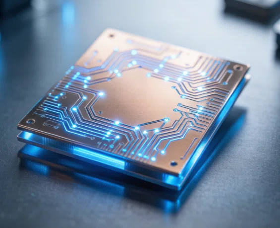
Regardless of the mechanism, through this microscopic processing using “light as a sculptor,” the originally uniform chemical film is perfectly sculpted at the molecular level with invisible circuit patterns identical to the design drawings.
Industrial-Grade Tier Balancing: The Balance Between Film Thickness Uniformity and Shelf Life
In the procurement specifications for presensitized PCB boards, two key performance indicators (KPIs) that severely test a board manufacturer’s supply chain capabilities are: absolute uniformity of the photosensitive film thickness and effective shelf life.
In practical use, photosensitive boards produced by many small workshops are frequently criticized by independent engineers overseas: “Why is it that the center of my board is completely developed, but the copper foil at the edges is still stuck with glue, and I can’t wash it off?”
The underlying technological flaw is the severely uneven thickness of the photosensitive adhesive on the copper-clad laminate surface.
If the photosensitive film at the edges is even just one micrometer thicker than in the center, then under the same UV exposure time and energy, the chemical molecules at the bottom of the edges cannot be completely “penetrated” or “broken down.” This leads to incomplete development, leaving a layer of microscopic glue residue.
Furthermore, because photosensitive films are composed of highly reactive diazo compounds or acrylate polymers, they undergo slow, self-heating cross-linking aging at room temperature. If warehouse management is poor or the container temperature during transport is too high, the photosensitive board will experience a “dark reaction.” Even without any light exposure, the entire board will become completely unusable after three months due to spontaneous hardening. Therefore, top-tier supply chain manufacturers must seal the boards in specially designed black moisture-proof and light-proof vacuum bags and forcibly store them in a cool, constant-temperature place below 22 degrees Celsius. This extreme protection of the material’s microscopic lifespan is the absolute dividing line between high-end materials and cheap, inferior products.
The Chemical Baptism of Development and Etching: Precision Circuitry Born in a Pot of Chemicals
After UV exposure, although the surface of the board already has invisible circuit patterns, it still needs two crucial chemical baptisms before it becomes a true circuit board: development and etching. These two steps require engineers to work in the lab, performing extremely precise operations in several different chemical solutions.
The millisecond-level game of development: making the invisible pattern instantly visible. The first step is development. Engineers prepare a very weak alkaline solution, typically around 1% concentration, most commonly anhydrous sodium carbonate (Na₂CO₃) or sodium silicate.
When the exposed presensitized PCB board is slowly immersed in the developing solution and gently shaken, a magical scene unfolds: the photosensitive film areas that were shattered by UV radiation in the first stage rapidly hydrolyze under the impact of the weakly alkaline water, turning into wisps of pale blue or green smoke that dissipates in the water, revealing the gleaming, exposed copper underneath. Meanwhile, the photosensitive film on the useful circuit areas, blocked by ink and untouched by UV radiation, exhibits extremely strong alkali resistance, clinging firmly to the copper surface like a sturdy shield, unmoved.
The development process is the most demanding “millisecond-level game” in the entire hand-made PCB manufacturing process, requiring the most manual experience. If the soaking time is insufficient (underdevelopment), a very thin, invisible monomolecular film will remain on the surface of the copper in the waste area. This will prevent the copper from dissolving during the subsequent acid pickling process, no matter how much strong acid is used, causing large-area micro-short circuits. If the soaking time is even slightly longer, even by thirty seconds (overdevelopment), the weakly alkaline liquid will capillarily penetrate along the edges of the useful traces, softening and peeling off the edges of the protective film that shouldn’t dissolve, resulting in incomplete traces and rendering the board unusable.
The Art of Environmental Etching: A Life-or-Death Battle Between Environmentally Friendly Ferric Chloride and High-Efficiency Hydrochloric Acid and Hydrogen Peroxide. After perfect development and rinsing with clean water, the board is immediately immersed in a second, more potent chemical solution—the etching solution. The sole purpose of etching is to completely dissolve and eliminate the unwanted exposed copper exposed during the development stage, leaving only the useful traces protected by the photosensitive dry film. In the manual environment of a laboratory, the supply chain primarily offers two mainstream etching solutions: Ferric chloride (FeCl3) saturated solution: This is the most traditional and safest classic solution. Ferric chloride reacts with metallic copper via a redox reaction of ferric ions, converting insoluble copper into soluble cupric chloride and ferrous chloride.
Its biggest advantage is its extremely mild reaction, with no release of corrosive or highly toxic gases. However, its disadvantages are also extremely frustrating: the liquid is a terrifying dark brown color, and if accidentally spilled on work clothes or the laboratory floor, it will leave permanent, indelible, burnt-yellow stains. Furthermore, its reaction speed is slow; the water must be heated to 50 degrees Celsius with a heating rod and constantly stirred with an air pump to complete the etching process within ten minutes. Hydrochloric acid (HCl) and hydrogen peroxide (H2O2) mixture: This is the most highly efficient “green solution” favored by modern laboratory geeks.
The mixture is transparent and clear, and the reaction speed is incredibly fast. The moment the board is placed in the solution, under the combined attack of the strong oxidizing agent hydrogen peroxide and the strong acid, the exposed copper turns from gold to transparent within two minutes, resulting in extremely clean and crisp trace edges. However, this method is a double-edged sword: the reaction releases chlorine gas and acid mist with a strong, pungent odor. Without a professional, powerful fume hood, this can cause severe chemical burns to the respiratory tract of operators.
The Impedance Hell of Manual Prototyping: How to Eliminate the “Jagged” Defects at Line Edges
After successfully obtaining shiny copper traces on the presensitized PCB board through development and etching, and wiping away any remaining photosensitive protective film with acetone, a true hardcore hardware engineer will immediately pick up a high-powered electron microscope to relentlessly examine the microscopic edges of these traces.
At this point, the most fatal and insurmountable hidden hell of hand-made PCBs is laid bare: microscopic “jaggedness” of the trace edges and severe “under-cut” defects.
Pixel Deception by Film Printers: Why Do Your Traces Look Like “Wavy Lines”?
Many beginners lacking high-frequency design experience, for convenience, use ordinary commercial laser printers or inkjet printers in the office when printing circuit diagram films.
The printed black film looks perfectly black. However, under ultraviolet light and the microscopic lattice, the printer is composed of discrete “toner particles” or “ink droplets.”
Under a high-powered microscope, the edges of lines that should be perfectly straight on the film are actually filled with countless dense, mosaic-like toner particle protrusions and depressions.
When ultraviolet light passes through these mosaic-edged films and shines onto the photosensitive plate, the light undergoes intense diffraction and scattering. This causes the molecules at the edges of the photosensitive film to break down, resulting in discontinuous, irregular serrated edges.
After further development and strong acid etching, the copper conductors remaining on the circuit board eventually become long, jagged, or wavy lines—terrifying microscopic burrs.
If the board is simply running a low-frequency 51 microcontroller or lighting a few LEDs, these jagged traces have no impact. However, if the customer’s board is handling X-band radar signals, high-speed DDR4/DDR5 memory buses, or high-frequency radio frequency traces at several gigahertz, these microscopic burrs become deadly sources of electromagnetic wave scattering.
Due to the skin effect, high-frequency currents only travel along the microscopic outer skin of the conductors. When it encounters these jagged burrs, the microscopic characteristic impedance of the traces undergoes wild, localized, disordered jumps. This causes severe reflections and significant return loss during signal transmission, resulting in a large-scale, instantaneous distortion of the signal waveform and ultimately, the complete collapse of high-frequency communication.
Ultimate Process Rescue Guide: Achieving Linewidth Miracles with High-Resolution Film and Weak Acid Spraying
To completely eradicate the hidden killers of high-frequency characteristics in a hand-operated laboratory environment, technical specifications typically guide high-end clients to upgrade the following two crucial process details:
Completely abandon toner printers and force an upgrade to “high-precision photoplotting film”: Film must be sent to a professional printing and typesetting shop for output using a specialized laser typesetting machine. The photosensitive silver halide particles in this film are at the nanometer scale, and their edge smoothness is three orders of magnitude higher than that of ordinary toner. This ensures that every cut made by UV light is an absolutely straight nanometer-level line, eliminating jagged edges at the source.
Abandon static soaking and introduce “heated weak acid atomized spraying process (Spray Etching)”: During the etching stage, never leave the board statically soaked at the bottom of the chemical bath. Because when the etching solution is still, it dissolves vertically downwards along the edge of the photosensitive film and then continues to hollow out laterally, causing severe “undercut,” resulting in traces that are wider at the top and narrower at the bottom, or even cutting the entire trace in half. Using a specialized hand-held spray machine, the warm etching solution is atomized into countless fine, high-pressure micro-streams, which bombard the board surface at high speed. Upon impact, the liquid carries away the dissolved copper ions instantly, preventing it from hollowing out laterally. This method can keep the undercut coefficient below 0.1, allowing for easy creation of ultra-fine, high-speed traces of 4 mils (0.1 mm) even by hand-fabrication.
The “Agile Fuel” for Global Makers, High-Energy Labs, and University R&D Supply Chains
Having thoroughly explained the material nature of presensitized PCB boards, the chemical hell of development and etching, and high-frequency impedance optimization, we now turn our attention to the macroscopic landscape of the electronics supply chain. While it doesn’t participate in the massive mass production of digital cameras or iPhones (often tens of millions of units), it is an indispensable “agile fuel” for research institutions, top university labs, and agile hardware startups during their R&D incubation phase.
A “Time Killer” for Shortening R&D Cycles
In the traditional New Product Introduction (NPI) process, after a hardware engineer designs a miniature RF filter or sensor interface circuit, they must package the Gerber file and send it to a professional PCB manufacturer. The manufacturer then has to go through more than ten rigorous industrial processes, including Engineering Evaluation (EQ), production scheduling, material cutting, electroplating, and solder masking. Even with the fastest super-fast expedited channel, it takes at least 24 to 48 hours from order placement to the delivery of the sample to the engineer’s desk.
Even more critically, if the engineer discovers during testing that a resistor-capacitor component’s package is misdesigned by a millimeter, or that a trace is missing, they must modify the design, reorder from the manufacturer, and wait another 24 hours. This lengthy waiting period is the most terrifying “time killer” in hardware R&D.
However, if lab shelves were stocked with presensitized PCB boards of various sizes, the entire story would be rewritten.
After discovering the error, engineers could modify the circuit diagram on their computers, and then immediately use nearby equipment to expose, develop, etch, and drill holes. The entire process would take only 20 minutes, resulting in a brand-new, improved prototype that could be soldered and tested on the spot. This terrifying agility—reducing the R&D iteration cycle from “days” to “minutes”—is a core strategic weapon for many research projects to be the first to publish papers in the international academic community, or for startups to launch their first-generation functional prototypes (MVPs) before their competitors.