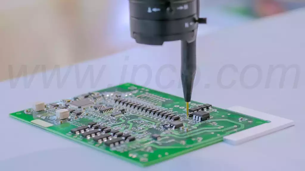
Among all components within the semiconductor test ecosystem, the ATE Load Board serves as the critical electrical bridge between the tester and the Device Under Test (DUT). While it may appear similar to a conventional PCB, its role extends far beyond providing physical connectivity.
A ATE Load Board must accurately transmit high-speed signals, deliver stable power, maintain measurement integrity, and withstand demanding production environments over extended periods of operation. Any weakness in its design can directly affect test accuracy, repeatability, throughput, and ultimately manufacturing yield.
Because of these requirements, ATE Load Board development is widely recognized as a specialized engineering discipline that combines signal integrity, power integrity, mechanical integration, thermal management, and reliability engineering into a single hardware platform.
Unique Design Challenges of ATE Load Boards
Unlike conventional electronic products, where PCB design primarily focuses on functionality and manufacturability, ATE Load Boards are developed with the objective of preserving electrical accuracy under highly dynamic testing conditions. As semiconductor devices become increasingly complex, the testing environment introduces several challenges that are rarely encountered in standard electronic applications.
One of the most common issues arises from the growing use of high-speed digital interfaces and high-frequency clock signals. Modern semiconductor devices often incorporate DDR memory channels, PCIe interfaces, high-speed ADCs, DACs, and SerDes architectures that operate at multi-gigabit data rates. Under these conditions, even minor impedance discontinuities, routing mismatches, or parasitic effects can generate reflections, crosstalk, and timing errors that compromise measurement accuracy.
Power delivery presents another significant challenge. Many advanced devices require multiple voltage domains and experience rapid current fluctuations during testing. If the power distribution network is not properly designed, voltage droop, switching noise, and transient instability may alter the DUT operating conditions, leading to inconsistent test results and yield variation.
Mechanical constraints also become increasingly difficult as device pin counts continue to rise. Higher-density packages create routing congestion, increase thermal concentration, and place greater demands on socket integration and fixture compatibility. In addition, major ATE platforms often employ different interface standards and mechanical configurations, making cross-platform compatibility an important consideration during the design process.
As a result, successful ATE Load Board development requires a comprehensive approach that balances electrical performance, mechanical reliability, and long-term production stability.
Signal Integrity Optimization for High Speed Testing
Signal integrity remains one of the most critical factors influencing Load Board performance. As interface frequencies continue to increase, maintaining clean and predictable signal transmission becomes essential for obtaining accurate test data.
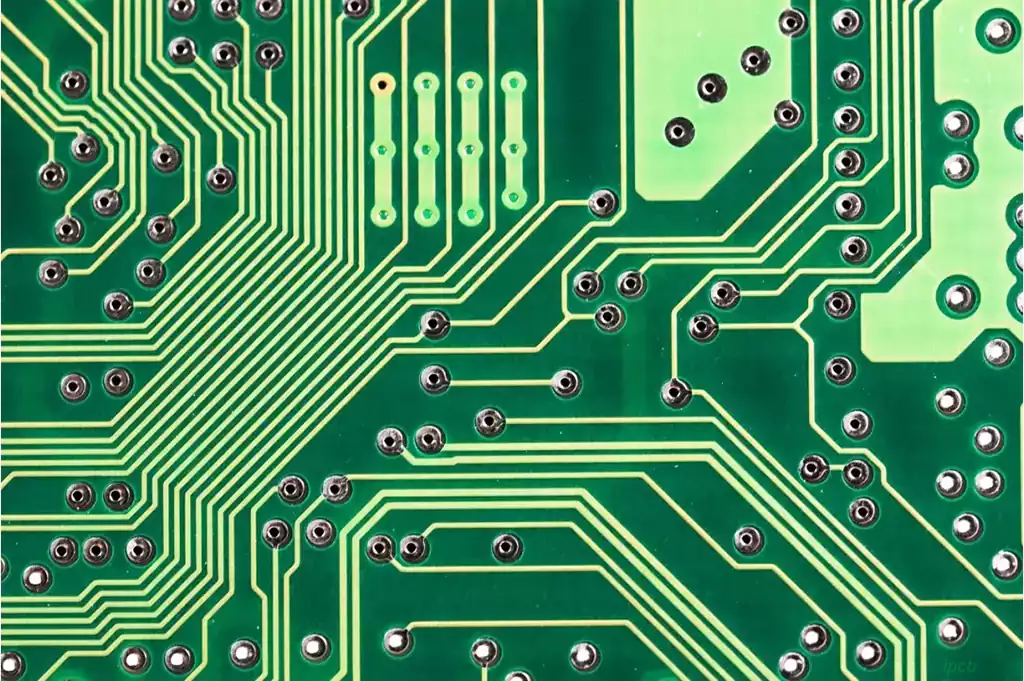
The foundation of signal integrity design begins with controlled impedance routing. High-speed signal paths must be designed to maintain consistent impedance characteristics throughout the transmission channel. Single-ended signals typically require 50-ohm impedance control, while differential interfaces commonly target 100-ohm differential impedance. Achieving these requirements demands careful consideration of PCB stack-up configuration, dielectric properties, trace geometry, conductor thickness, and layer arrangement. Any abrupt changes in these parameters can introduce reflections and degrade waveform quality.
Beyond impedance control, routing topology plays a major role in reducing signal degradation. High-speed channels should be physically isolated from low-speed control circuits and noisy power networks whenever possible. Differential pairs require tight length matching and consistent spacing to minimize timing skew and maintain signal synchronization. Continuous ground reference planes provide stable return paths and help suppress electromagnetic coupling between adjacent traces.
Via design is equally important. Although vias are often unavoidable in complex layouts, excessive via transitions introduce parasitic capacitance and inductance that can negatively impact high-frequency performance. Designers typically minimize unnecessary layer changes, optimize via geometry, and shorten critical signal paths to reduce these effects. For particularly sensitive interfaces, carefully selected termination schemes can further improve signal quality by reducing overshoot, undershoot, and ringing.
When these design principles are applied together, the resulting transmission channel can maintain signal fidelity throughout the testing process, enabling accurate characterization of advanced semiconductor devices.
Power Integrity and PDN Architecture
While signal integrity often receives the greatest attention, power integrity is equally important in achieving reliable semiconductor testing. In many production environments, inconsistent test results can be traced directly to deficiencies within the power delivery system rather than the DUT itself.
The primary objective of power integrity design is to create a low-impedance Power Distribution Network (PDN) capable of delivering stable voltage under varying load conditions. This is typically achieved through a combination of dedicated power planes, wider copper traces, thicker copper weights, and strategically placed via arrays. By reducing both resistive and inductive losses, the PDN can maintain stable voltage levels even during periods of rapid current demand.
Noise suppression is another essential aspect of power system design. Because power disturbances occur across a wide frequency spectrum, a single capacitor type cannot effectively address all noise sources. Designers therefore employ multi-stage decoupling strategies that combine bulk capacitors for low-frequency filtering with ceramic capacitors for high-frequency suppression. Placing these components as close as possible to the DUT power pins minimizes loop inductance and improves transient response.
As semiconductor devices increasingly integrate analog, digital, and RF subsystems, power domain isolation also becomes critical. Separate power regions and return paths help prevent digital switching noise from coupling into sensitive analog measurement circuits. This isolation improves the accuracy of precision measurements involving voltage, current consumption, gain, linearity, and noise performance.
Together, these power integrity practices help establish stable operating conditions throughout the testing process and significantly improve measurement repeatability.
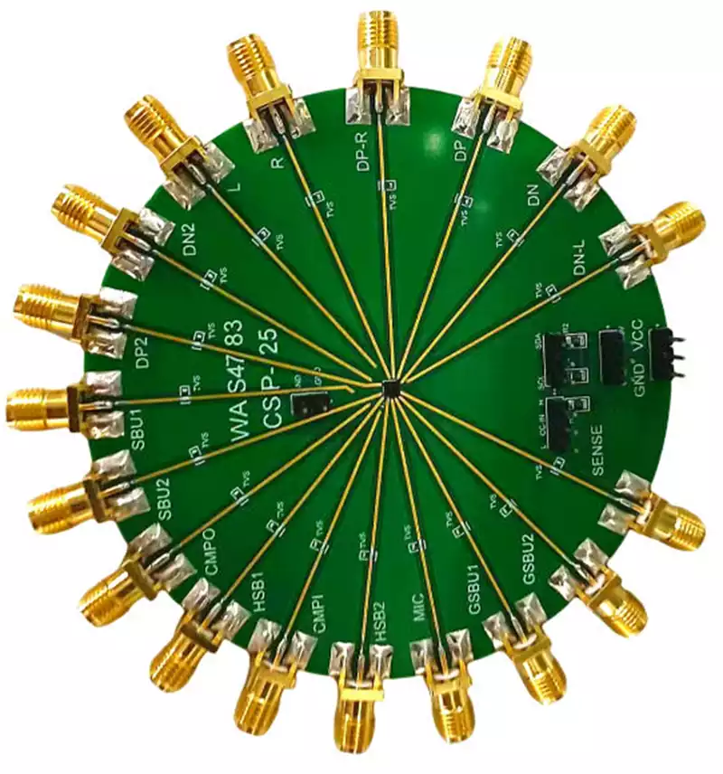
Mechanical Compatibility and Test Fixture Integration
Electrical performance alone cannot guarantee a successful ATE Load Board design. The board must also integrate seamlessly with the physical testing environment, including sockets, fixtures, handlers, and ATE systems.
Most semiconductor test facilities operate equipment from multiple vendors, such as Teradyne, Advantest, and Chroma. Each platform may employ unique connector arrangements, mounting requirements, and interface standards. Designing with platform compatibility in mind can significantly reduce engineering revisions and accelerate deployment schedules.
Socket integration represents another important consideration. Modern semiconductor packages such as BGA, QFN, LGA, and CSP devices require precise mechanical alignment to ensure consistent electrical contact. Even slight positioning errors can lead to intermittent failures, unstable measurements, or reduced test yield. Consequently, socket selection, mounting tolerances, and pad design must be carefully coordinated during the development process.
Thermal and mechanical factors must also be evaluated simultaneously. Component placement should account for fixture clearance requirements, airflow pathways, heat dissipation needs, and material expansion characteristics. Proper mechanical planning helps prevent assembly interference, minimizes stress concentrations, and improves long-term operational stability.

Reliability Considerations for High Volume Production Testing
Unlike engineering evaluation boards that may only be used for limited validation work, production ATE Load Boards are expected to operate continuously through hundreds of thousands or even millions of test cycles. This demanding environment makes reliability one of the most important design priorities.
Material selection plays a crucial role in long-term performance. High-frequency applications often require low-loss laminates with stable dielectric properties across a broad temperature range, while high-current applications benefit from materials that offer enhanced thermal conductivity and current-carrying capability. Selecting appropriate substrate materials helps maintain consistent electrical performance throughout the product lifecycle.
Component reliability is equally important. Industrial-grade passive components, connectors, and sockets are commonly used to withstand extended production operation and repeated insertion cycles. These components provide improved durability and reduce the risk of unexpected failures during high-volume manufacturing.
Thermal management must also be considered from the earliest design stages. Power-intensive devices generate significant heat during testing, and insufficient thermal capacity can accelerate material degradation and reduce system reliability. By incorporating adequate cooling paths, current-carrying margin, and thermal spacing, engineers can ensure stable performance over long operating periods.
In addition, incorporating diagnostic features such as test points, tuning locations, and debugging interfaces can simplify maintenance and future optimization efforts. These features often reduce downtime and lower overall operational costs during production.
Common Design Pitfalls and Engineering Recommendations
Despite advances in simulation tools and PCB design technologies, several common mistakes continue to affect ATE Load Board performance. One of the most frequent issues is the failure to perform comprehensive signal integrity and power integrity analysis during the design stage. Problems such as waveform distortion, excessive noise, and timing violations may not become apparent until hardware testing begins, at which point corrective actions can be both time-consuming and expensive.
Another recurring challenge involves inadequate partitioning between analog circuits, digital logic, high-speed interfaces, and power distribution networks. Without proper separation, unwanted coupling and electromagnetic interference can significantly reduce measurement accuracy.
Cost-driven material selection also creates problems in some projects. While lower-cost PCB materials may reduce initial manufacturing expenses, they often exhibit greater thermal drift and higher losses under demanding operating conditions, ultimately compromising long-term stability and test consistency.
Mechanical tolerances are sometimes overlooked as well. Insufficient consideration of socket alignment, fixture integration, or assembly tolerances can lead to contact failures, increased maintenance requirements, and reduced testing efficiency.
Recognizing and addressing these issues early in the design cycle can significantly improve overall project success and reduce total development cost.
ATE Load Board design is far more than a conventional PCB development task. It is a multidisciplinary engineering effort that requires careful coordination of high-speed signal transmission, power delivery architecture, mechanical integration, thermal management, and reliability planning.
Although many design choices may appear insignificant at the board level, their impact becomes substantial when multiplied across millions of semiconductor devices and countless production test cycles. A carefully engineered ATE Load Board can improve measurement accuracy, enhance yield performance, reduce operational costs, and accelerate time-to-market.