Smartphone PCB layout is widely regarded as one of the most challenging aspects of product design. Under the dual constraints of ultra-thin form factors and increasingly powerful hardware, designers must contend with extremely limited board space, escalating component density, and growing signal integrity concerns. As a result, PCB layout has evolved far beyond conventional circuit placement and routing into a highly sophisticated system-level engineering discipline.
Core Design Challenges in Smartphone PCB Layout
The rapid evolution of mobile communication technologies has transformed mobile phones from basic devices capable of voice calls and simple timekeeping into multimedia terminals supporting audio and video playback, high-resolution photography, gaming, and, ultimately, today’s smartphones equipped with advanced operating systems, third-party application ecosystems, and ubiquitous wireless connectivity. Modern smartphones have long surpassed their original role as communication tools and have become indispensable intelligent devices for work, entertainment, and everyday life.
As smartphone functionality continues to expand and user expectations rise, industrial design requirements have become increasingly demanding. Slimmer profiles, integrated structures, and refined aesthetics have become the norm. As the primary carrier of electronic components and electrical interconnections, the PCB must accommodate these trends toward miniaturization and lightweight construction, creating a series of significant layout challenges. The complexity of smartphone PCB design continues to increase exponentially, primarily across the following five dimensions.
Extreme Miniaturization and Space Constraints
The ongoing reduction in smartphone thickness and overall dimensions requires continuous decreases in PCB size and substrate thickness. Consequently, the physical area available for component placement and signal routing becomes increasingly limited, significantly reducing layout tolerance and design flexibility.
High Component Density Driven by Functional Integration
Modern smartphones integrate a wide range of functions, including cellular communications, high-definition multimedia processing, AI computing, environmental sensing, and satellite or GNSS positioning. This extensive functional integration dramatically increases component count and board-level density, making congestion, routing conflicts, and placement optimization increasingly challenging.
Advanced Packaging Requirements
As smartphone performance continues to improve, critical devices such as application processors, RF transceivers, and memory chips feature higher pin counts and increasingly compact package geometries. These advanced packages place stringent demands on placement accuracy, alignment precision, and spacing control, far exceeding the requirements of traditional electronic products.
Signal Integrity Challenges in High-Speed and High-Frequency Designs
The widespread adoption of technologies such as 5G connectivity, 4K displays, high-speed flash storage, and high-resolution image transmission has substantially increased the proportion of high-frequency and high-speed signals on smartphone PCBs. These signals are highly sensitive to routing length, path topology, and surrounding electromagnetic conditions. Even minor layout deviations can result in signal attenuation, distortion, reflection, and transmission degradation.
Electromagnetic Interference Among Mixed-Signal Systems
Within the confined area of a smartphone PCB, high-power supply circuits, digital logic signals, analog audio and sensor circuits, and RF communication systems coexist in close proximity. The significant differences in frequency, voltage, and power characteristics among these signal types create substantial risks of crosstalk and electromagnetic interference (EMI), making interference mitigation increasingly difficult.
The combined impact of these challenges elevates smartphone PCB layout from a conventional circuit design task to a highly precise and complex systems engineering project. Designers must possess a strong foundation in circuit design, understand the layout requirements of individual functional modules, and be proficient in industry-standard EDA platforms such as Mentor Xpedition and PADS. By leveraging component specifications from semiconductor vendors such as Texas Instruments and integrating 3D mechanical CAD collaboration tools, engineers can achieve seamless coordination between electronic circuitry and mechanical structures, ensuring compliance, stability, and manufacturing efficiency.
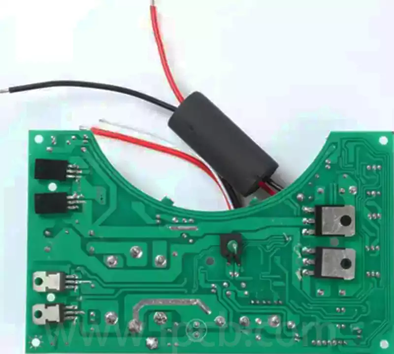
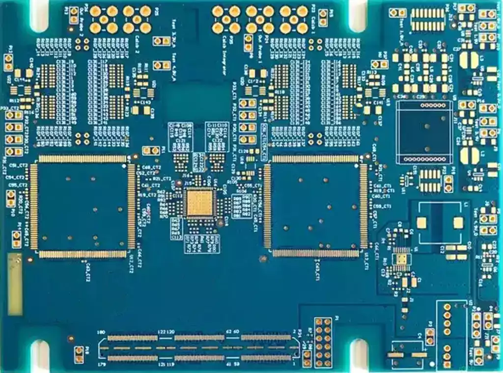
Component placement is the foundation of smartphone PCB design. Its quality directly affects signal integrity, power distribution stability, and thermal performance. Owing to its technical complexity and precision requirements, PCB layout consistently represents one of the most time-consuming stages in the smartphone development process.
Core Design Principles for Smartphone PCB Layout
1.Balanced Center-of-Gravity Distribution
Components should be distributed as evenly as possible to maintain a balanced center of gravity across the PCB. This helps prevent board warpage and deformation while ensuring structural stability during assembly and operation.
2.Organized and Consistent Placement
Components belonging to the same functional category should be aligned and oriented consistently. A clean and orderly layout improves space utilization, facilitates mass production, simplifies inspection and troubleshooting, and reduces manufacturing and maintenance costs.
3.Shortest Signal Path Principle
Critical signal paths, particularly high-speed interfaces such as DDR, LVDS, and MIPI, should be optimized for minimum routing length and minimal discontinuities. Straight and direct routing reduces transmission loss, signal degradation, and timing-related issues.
4.Physical Isolation of Power and Sensitive Circuits
High-voltage and high-current power circuits, such as battery supply and DC-DC converter outputs, should be physically separated from low-voltage and low-current RF circuits. Proper partitioning minimizes electromagnetic interference and ensures reliable wireless communication performance.
5.Digital and Analog Partitioning
Digital subsystems, including DDR memory, LVDS display interfaces, MIPI channels, and baseband processing circuits, should be grouped separately from analog circuits such as audio and RF modules. Effective partitioning minimizes digital-to-analog interference and improves signal purity.
6.Separation of High-Frequency and Low-Frequency Circuits
Given their strong radiation characteristics and susceptibility to interference, high-frequency circuits should maintain adequate spacing from low-frequency circuits. This strategy complements digital-analog partitioning and further reduces unwanted coupling effects.
7.Independent Signal Return Paths
Each functional subsystem should maintain a complete and independent signal return loop. Overlapping or shared return paths can introduce reflections, crosstalk, and impedance discontinuities.
8.Manufacturing-Oriented Component Orientation
Through-hole and surface-mount devices should follow consistent placement orientations along the X or Y axis. Polarized components, such as capacitors and diodes, should maintain uniform polarity direction to support automated assembly processes and simplify maintenance.
9.Adequate Component Spacing
Component spacing should be planned carefully. Large devices should not be placed too close to miniature precision components. Adjustable circuits and impedance-matching networks should be allocated sufficient access space for tuning, debugging, and servicing.
10.Distributed Thermal Management
High-power heat-generating devices, such as PMICs and charging management ICs, should be distributed across the PCB rather than concentrated in a single area. This promotes uniform heat dissipation and prevents localized overheating.
11.Thermal Protection for Temperature-Sensitive Devices
Except for dedicated temperature sensors, thermally sensitive components should be positioned away from major heat sources to prevent performance degradation and reduced service life.
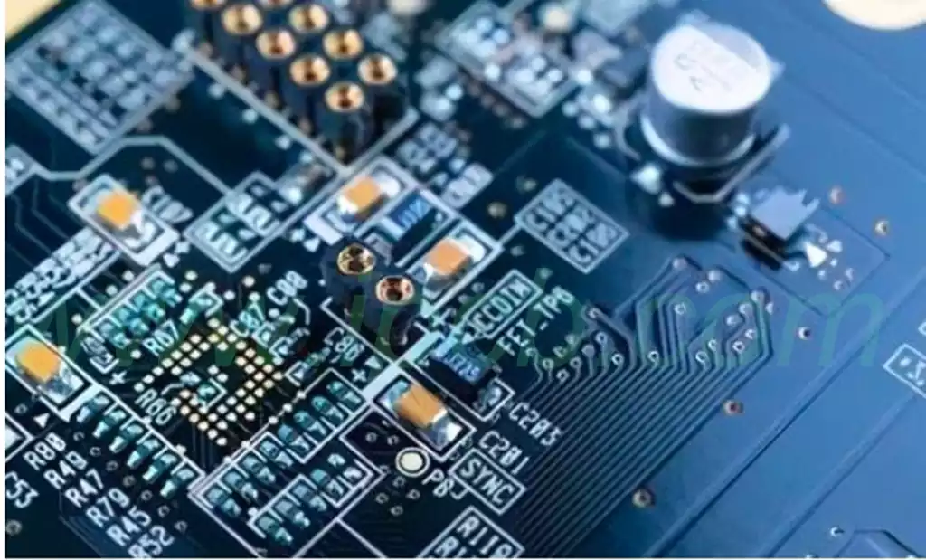
12.Proximity Placement of Decoupling Capacitors
Power decoupling capacitors should be located as close as possible to the corresponding IC power pins. Minimizing loop inductance enables rapid suppression of voltage fluctuations and high-frequency noise, ensuring stable power delivery.
13.Grouping by Power Domain
Components operating from the same power rail should be placed within the same functional region. This simplifies power distribution network design and enhances overall power integrity.
14.Accurate Impedance Matching
Termination and matching components should be positioned according to signal transmission requirements. Series termination resistors should be placed close to the signal source, typically within 500 mils. For multi-load signal networks, termination devices should be located at the far end of the transmission path to ensure proper impedance matching and eliminate signal reflections.
Fundamental Layout Methodology for Smartphone PCBs
After defining design challenges and layout principles, engineers must establish a systematic layout strategy rather than relying on fragmented or ad hoc placement decisions. Smartphone PCB layout should be guided by the circuit block diagram and follow the primary signal flow throughout the system.
A fundamental rule is to follow the principle of “large before small, difficult before easy.” Critical functional blocks such as the application processor, power management circuitry, and RF subsystems should be placed first, followed by smaller passive and support components. Likewise, high-speed, high-density, and impedance-sensitive circuits should be addressed before routine functional modules.
Taking a smartphone platform based on the Qualcomm MSM8xxx series as an example, a standardized layout methodology can be illustrated. The platform features a low-power octa-core 2.2 GHz processor fabricated using a 14 nm process, providing an effective balance between computational performance and power efficiency. It is paired with 32 GB of eMMC flash storage and 16 GB of LPDDR3 memory to support multitasking and large-capacity data storage.
The power management architecture employs a dual-chip solution consisting of the PM8953 and PMI8952. The PM8953 handles core system power distribution and audio processing functions, serving as the primary power management controller. The PMI8952 focuses on specialized power functions, including battery charging management, power-path control, display backlight driving, flash LED control, LCD bias generation, and motor drive support. Together, these devices deliver comprehensive and highly accurate power management for the entire smartphone system.
The RF and wireless subsystem incorporates the WTR2965 RF transceiver, supporting 4G+ network standards and dual-SIM dual-standby functionality. The WCN3680 connectivity chip integrates Wi-Fi, Bluetooth, and FM radio capabilities, delivering high-throughput wireless performance while maintaining low power consumption.
For imaging and display applications, the platform supports a multi-camera configuration consisting of a 13 MP + 5 MP rear camera system and an 8 MP front-facing camera. Display functionality is provided through a 6-inch Full HD touchscreen panel, balancing visual quality and touch responsiveness.
Subsequent layout optimization focuses on five major subsystems—power management, application processing, RF communications, imaging, and display circuitry. By carefully applying dedicated placement strategies to each functional block, designers can maximize system performance while ensuring reliability and manufacturability.
At its core, smartphone PCB layout is a process of balancing performance, manufacturability, and reliability within an extremely constrained physical space. From signal integrity and thermal management to analog-digital partitioning and electromagnetic interference control, every placement decision directly influences the final product’s performance. A well-executed layout not only ensures stable operation and regulatory compliance but also forms the foundation for delivering the user experience expected from modern smartphones.