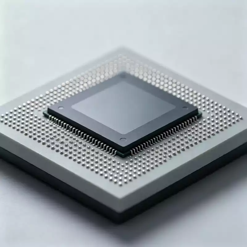
Flip Chip (FC), also known as flip chip packaging, is one of the most widely used advanced semiconductor packaging technologies in the industry. Unlike conventional wire bonding, Flip Chip technology mounts the active surface of the semiconductor die face-down onto a substrate or package carrier. Instead of using bonding wires to establish electrical connections, solder bumps are fabricated directly on the chip’s bond pads.
The die is then flipped, precisely aligned with the corresponding pads on the substrate, and joined through a reflow soldering process. This approach simultaneously provides reliable electrical interconnection and strong mechanical attachment between the chip and the substrate, while significantly shortening the signal transmission path and improving package performance.
The complete Flip Chip packaging process is highly sophisticated and requires extremely tight process control throughout manufacturing. A typical production flow includes incoming wafer inspection, substrate preparation, bump fabrication, wafer thinning through back grinding, wafer dicing, flip chip bonding, underfill dispensing, adhesive curing, molding, laser marking, solder ball attachment, final package sorting, and comprehensive electrical and reliability testing. Every manufacturing stage directly influences package yield, product reliability, and long-term service life, making process precision essential for advanced semiconductor packaging.
Among all Flip Chip manufacturing processes, bump fabrication is one of the most critical steps because the dimensional accuracy, structural integrity, and long-term stability of the bumps determine the overall reliability of the chip interconnection system. Today, four bump structures dominate high-volume semiconductor manufacturing: Controlled Collapse Chip Connection (C4) solder bumps, copper pillar bumps, copper pillar bumps with solder caps, and copper-to-copper (Cu-Cu) hybrid bonding structures.
The C4 process, originally developed by IBM, is regarded as the landmark technology that enabled the commercial adoption of Flip Chip packaging. In this process, an Under Bump Metallization (UBM) layer is first deposited on the chip bond pads using Physical Vapor Deposition (PVD). The UBM serves several essential functions by providing strong adhesion between the bump and the bond pad, preventing metal diffusion between different materials, and promoting proper solder wetting during reflow.
This metallization layer is fundamental to maintaining a reliable metallurgical interface and preventing interfacial delamination throughout the product’s service life. Once the UBM has been formed, the solder layer can be produced by vacuum evaporation, stencil printing, electroplating, or other fabrication methods. The chip is then flipped, accurately aligned with the substrate, and electrically interconnected through the reflow soldering process. For many years, this represented the standard manufacturing method for mass-producing Flip Chip packages with solder bumps.
As semiconductor packaging technology has continued to evolve, electroplating has gradually replaced many traditional bump fabrication methods because of its superior precision, excellent process consistency, and outstanding compatibility with advanced packaging requirements. Electroplating supports the high-volume production of both solder bumps and copper pillar bumps while meeting the increasingly demanding requirements of ultra-fine-pitch interconnections and large-diameter wafers. For this reason, it has become the mainstream bump fabrication technology used in today’s advanced semiconductor packaging industry.
Solder bumps were the earliest and most widely adopted interconnection structure in Flip Chip packaging. Their manufacturing process involves depositing a relatively thick solder layer on top of an ultra-thin UBM layer, allowing the solder to melt during reflow and form both the electrical and mechanical connections between the chip and the substrate. Because the process is well established, relatively easy to manufacture, capable of delivering high production yields, and proven to provide stable long-term reliability, solder bump technology remained the industry’s preferred solution for many years.
However, conventional solder bumps also have inherent limitations. Since the solder melts completely during reflow, maintaining consistent bump height across the entire package becomes increasingly difficult. As bump pitch continues to shrink, adjacent solder bumps become more susceptible to bridging during reflow, creating electrical short circuits that reduce manufacturing yield and package reliability. These limitations make traditional solder bumps unsuitable for the ultra-fine-pitch layouts required by today’s highly integrated semiconductor devices, leading the industry to adopt more advanced bump structures.
Compared with conventional solder bumps, copper pillar bumps maintain their structural geometry during the soldering process because the copper pillar itself does not melt during reflow. This characteristic fundamentally overcomes the pitch limitations associated with solder bumps and enables significantly finer bump pitches together with much higher I/O density. Copper pillar technology also offers superior electrical conductivity, improved thermal dissipation, greater mechanical reliability under long-term operating conditions, and better manufacturing cost efficiency in high-volume production. As semiconductor devices continue to evolve toward higher integration, greater I/O counts, and smaller package sizes, the packaging industry is rapidly transitioning to ultra-fine-pitch copper pillar technology as the preferred interconnection solution for next-generation Flip Chip packaging.
Complete Copper Pillar Bump Fabrication and Flip Chip Bonding Process
1.Polyimide (PI) Coating
Copper pillar bumps are rigid three-dimensional structures. If they are fabricated directly on the wafer surface, they generate continuous mechanical stress that may cause wafer deformation, structural cracking, or device failure during both manufacturing and long-term operation. To absorb this stress, protect the wafer substrate, and improve overall package reliability, a polyimide (PI) coating process is performed before bump fabrication. A uniform layer of flexible polyimide film is applied across the wafer surface to act as a stress buffer, reducing the mechanical load introduced by the copper pillars while maintaining the structural integrity of the wafer and providing a stable foundation for the subsequent fabrication processes.
2.Under Bump Metallization (UBM) Deposition
The purpose of the UBM process is to form a dual-layer structure consisting of a diffusion barrier layer and a conductive seed layer using physical vapor deposition (PVD). First, a barrier layer made of titanium (Ti) or titanium tungsten (TiW) is deposited onto the chip pads. This layer effectively prevents atomic diffusion between the silicon substrate and the subsequent copper layer, thereby eliminating electrical failures caused by metal migration. A pure copper (Cu) seed layer is then deposited on top of the barrier layer. The seed layer provides a uniform conductive surface for the electroplating process while strengthening the adhesion between the different metal layers and preventing delamination during subsequent manufacturing steps.
3.Photolithography
Photolithography is performed to create precise plating molds that define the size and location of each copper pillar bump. The process begins with argon plasma cleaning to completely remove oxide films, dust particles, and other contaminants from the wafer surface, ensuring an exceptionally clean substrate. A layer of photoresist is then spin-coated onto the wafer at high speed, followed by soft baking, precise mask alignment, ultraviolet exposure, and development. These steps produce photoresist openings that accurately match the intended bump dimensions and layout, providing a highly precise template for the subsequent electroplating process.
4.Multilayer Metal Electroplating
Electroplating is the core process used to form the copper pillar bump structure. After the wafer has been mounted on a dedicated electroplating fixture, it is immersed in a copper plating solution. By precisely controlling parameters such as plating time, current density, solution temperature, flow rate, and electrolyte composition, copper is deposited within the photoresist openings to form copper pillars with the required height and geometry. Once the copper pillars have been completed, a nickel (Ni) layer is electroplated as a diffusion barrier and protective layer to improve structural stability and oxidation resistance. Finally, a tin-based solder layer is electroplated onto the top of each copper pillar, completing the entire bump structure.
5.Wafer Cleaning and Photoresist Removal
Following electroplating, the wafer surface contains residual plating chemicals, metal particles, and hardened photoresist. These contaminants are removed using professional wafer cleaning equipment to restore a clean processing surface. A chemical stripping process is then carried out to completely remove the remaining photoresist. This ensures that both the wafer surface and the copper pillar bumps are free of contamination before the etching and bonding processes, thereby preventing impurities from affecting manufacturing accuracy or package reliability.
6.UBM Etching
The objective of the UBM etching process is to electrically isolate each individual copper pillar bump by removing the exposed UBM material between adjacent bumps. During etching, both the etching area and depth must be precisely controlled so that only the uncovered UBM is removed while the functional UBM directly beneath each copper pillar remains intact. Insufficient etching may leave conductive metal bridges that cause electrical short circuits, whereas excessive etching may damage the base of the copper pillars, weaken the bump structure, and reduce the long-term reliability of the finished package.
7.Reflow Pre-Treatment
After UBM etching, the wafer undergoes a reflow pre-treatment process inside a temperature-controlled reflow oven. During reflow, the tin solder cap on each copper pillar melts uniformly and reacts metallurgically with the underlying copper, forming stable intermetallic compounds (IMCs). As the solder solidifies during cooling, it creates a highly conductive and mechanically robust bonding interface. Throughout this process, critical parameters including peak temperature, heating rate, and dwell time must be carefully controlled to regulate the thickness and morphology of the IMC layer, ensuring excellent electrical performance and long-term joint reliability.
8.Flip Chip Assembly
Flip chip assembly is the final and most critical stage of the packaging process. The die carrying the completed copper pillar bumps is accurately flipped and aligned so that every bump corresponds precisely to its designated pad on the substrate. The assembly then undergoes a second reflow soldering process, during which metallurgical bonds are formed between the copper pillar bumps and the substrate pads. This process simultaneously establishes reliable electrical interconnections and strong mechanical attachment between the chip and the substrate, completing the entire flip chip packaging process.
Compared with conventional solder bump flip chip packaging, copper pillar bump technology offers significant performance advantages. In addition to enabling ultra-high I/O density and ultra-fine-pitch interconnections, it substantially improves both the electrical and thermal performance of the chip, resulting in greater reliability under prolonged high-temperature and high-load operating conditions. Furthermore, the process supports lead-free mass production, fully complying with the environmental requirements of the modern electronics industry. These advantages have made copper pillar flip chip packaging one of the preferred solutions for advanced semiconductor device packaging.
As semiconductor packaging technology continues to evolve, flip chip packaging is also undergoing continuous refinement and innovation. Ongoing advancements in materials, bump structures, and manufacturing processes are further enhancing package performance, reliability, and integration density. With its outstanding electrical performance, excellent thermal management capability, and compatibility with next-generation high-density devices, advanced flip chip packaging is expected to remain one of the dominant technologies in high-end semiconductor packaging for the foreseeable future.