In high-power industrial power supplies, new energy vehicle powertrains, server power modules, and motor drive control systems, high current circuit boards play a crucial and unique role. Traditional circuit boards primarily focus on transmitting weak electrical signals and logic control, typically carrying currents in the milliampere to ampere range. High-current circuit boards, however, must safely, stably, and efficiently guide continuous or pulsed currents of tens, hundreds, or even thousands of amperes while transmitting high-density control signals.
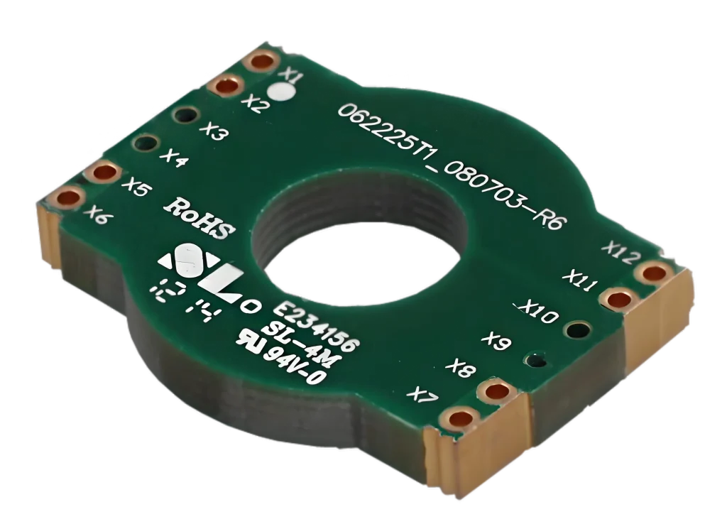
This enormous current load transforms the circuit board from a simple conductor carrier into a complex nonlinear three-dimensional system involving microscopic heat conduction, electromagnetics, material aging, and parasitic inductance tuning. When hundreds or thousands of amperes of electrons flow through micrometer-scale copper foil and vias, even minute differences in resistance and impedance are converted into intense Joule heating, posing a severe challenge to the insulating medium, solder interfaces, and substrate structure.
To construct a high-current circuit board that is as stable as steel, possessing both ultra-high energy density and extremely low failure risk, the hardware engineering team must deeply dissect its current-carrying mechanism, thermal resistance network, ground plane return current control, and micro-fabrication implementation from the perspectives of fundamental physics and materials science.
Microscopic Conductors and Thermodynamic Limits: The Physical Mechanism of High-Current Current Carrying
Before discussing the design of a high-current circuit board, a profound understanding of the microscopic physical properties of copper conductors is essential. Although copper, as the primary conductive medium in printed circuit boards, has extremely high conductivity, its inherent resistive characteristics still lead to significant energy losses when high currents pass through it. These losses are invariably converted into heat energy.
Joule Heating Effect and the Nonlinear Equilibrium of Copper Foil Temperature Rise
When current flows through the copper foil traces on the circuit board, electrons move directionally under the influence of the electric field and frequently collide with atoms in the copper lattice. This microscopic collision converts kinetic energy into heat energy from lattice vibrations, i.e., Joule heating.
For a high-current circuit board, the temperature rise of the copper traces is a dynamic thermal equilibrium process. On one hand, traces continuously generate heat due to Joule heating; on the other hand, this heat dissipates to the surrounding environment through conduction, convection, and radiation. If the generated heat exceeds the dissipated heat, the trace temperature will continue to rise.
Copper’s resistivity is not constant; it has a positive temperature coefficient. This means that as the temperature rises, the resistance of the copper conductor increases further, generating even more heat. If the heat dissipation design of a high-current circuit board is inadequate, the traces may fall into a vicious cycle of rising temperature, increased resistance, and intensified heat generation, ultimately leading to glass transition temperature failure of the substrate, resin yellowing and peeling, or even direct melting of the copper foil.
The Physical Evolution of Copper Foil Thickness: From Conventional Copper to Ultra-Heavy Copper Processes
To solve the severe heat generation and voltage drop problems caused by high current, the most direct and effective means is to increase the cross-sectional area of the conductor. In traditional circuit board designs, a copper thickness of one ounce (approximately 35 micrometers thick) or two ounces (approximately 70 micrometers thick) is sufficient for most signal boards. However, in high-current circuit boards facing hundreds of amperes of current carrying capacity, such thickness is extremely fragile.
Modern high-power, high-current circuit boards widely employ ultra-heavy copper processes ranging from three to ten ounces or more, with some highly specialized industrial and automotive-grade circuit boards even using copper layers exceeding twenty ounces.
This heavy copper process not only significantly enlarges the cross-sectional area of the traces, drastically reducing electrical resistance, but also greatly expands the horizontal heat sink volume of the circuit board. Heat can rapidly dissipate along the thick copper layer, preventing the formation of localized hot spots.
However, the ultra-heavy copper process also presents severe microphysical challenges to circuit board manufacturing. With the significant increase in copper thickness, side etching becomes extremely severe, causing the trace cross-section to no longer be an ideal rectangle, but rather trapezoidal or even with significant grooves. This necessitates a readjustment of the physical limits of minimum trace width and spacing during the manufacturing of high-current circuit boards, and the use of more adhesive during lamination to prevent microscopic bubbles and dielectric voids at the edges of the ultra-thick copper traces.
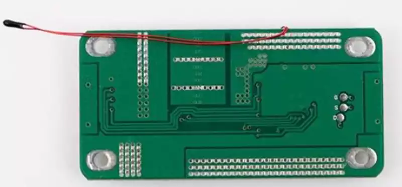
The introduction of surface-mount copper venting and soldering, along with metal substrates, is another highly efficient physical method to enhance current-carrying capacity, besides simply increasing the thickness of inner and outer copper foil layers.
On high-current circuit boards, engineers specifically remove solder resist to expose the underlying pure copper. During subsequent assembly and soldering, a layer of solder alloy, ranging from 0.5 mm to over 1 mm thick, is fused and solidified in the vented area. Although the conductivity of solder itself is significantly lower than that of pure copper, its thickness is dozens of times greater, resulting in an order-of-magnitude increase in the overall cross-sectional area. This drastically reduces the equivalent impedance of the traces, multiplying their rated current-carrying capacity.
When the current density further exceeds the thermal conductivity limit of organic insulating substrates (such as traditional fiberglass epoxy), high-current circuit boards must shift to metal substrates (such as aluminum or copper substrates) or ceramic substrates.
A metal substrate, by bonding an ultra-thin, high-thermal-conductivity insulating layer between a metal base plate and copper foil, instantly and vertically conducts the heat generated by high-current power devices to the underlying metal block, from which it is then dissipated by an external heat sink. This structure reduces the thermal resistance of traditional circuit boards by several orders of magnitude, enabling the board to operate stably under extremely harsh high-temperature, high-current environments.
Three-Dimensional Microscopic Heat Conduction: Thermal Via Networks and Thermal Stress Management
In high-current circuit boards, heat transfer is not merely a two-dimensional process, but a complex three-dimensional heat conduction process. Many high-current power devices (such as surface-mount power MOSFETs or insulated-gate bipolar transistors) are tiny in size but require the instantaneous flow of tens or even hundreds of amperes of current. The substrate beneath these devices becomes a microscopic hotspot for concentrated heat generation.
How to efficiently guide and disperse this intense Joule heat concentrated in a point-like area to various physical layers of the circuit board and even the external environment is a central challenge in the thermodynamic design of high-current circuit boards.
Thermal Via Geometry and Copper Plating Thickness Control
In multilayer high-current circuit board design, vertical heat conduction primarily relies on an array of thermal vias that penetrate between the copper layers.
A via is physically a hollow copper cylinder. When heat is conducted from the pads of upper-layer power devices to the via, the heat flow mainly follows the copper plating layer on the via wall downwards. Therefore, the thermal conductivity of a thermal via directly depends on the microscopic thickness of the copper plating layer.
In conventional circuit board manufacturing, the copper plating thickness of via walls is typically only around 20 micrometers. However, in high-standard high-current circuit boards, higher process specifications are required for the via wall plating, demanding copper thicknesses of 30 micrometers or even 45 micrometers or more.
Simultaneously, the geometric diameter of thermal vias involves an extremely delicate physical balance. While excessively large via diameters (e.g., greater than 0.5 mm) increase the cross-sectional area of the plated copper, they can cause severe capillary desoldering during reflow soldering, drawing away solder intended for the power device base and creating large air voids within the pads. Since air has extremely low thermal conductivity, this effectively creates a break in the heat conduction path. Conversely, excessively small via diameters can hinder plating penetration, resulting in uneven plating on the via walls.
Therefore, the via diameter of high-performance high-current circuit boards should be strictly controlled between 0.2 mm and 0.35 mm, using a high-density matrix distribution, with the via center-to-center distance controlled at approximately 0.8 mm. This creates a highly efficient three-dimensional thermally conductive copper pillar forest directly beneath the power devices.
Resin-Plug Through-Pad and Through-Pad Plating Smoothing Process
To completely resolve the contradiction of solder absorption by hot vias causing pad voids, modern high-end high-current circuit boards widely employ through-pad and thermally conductive resin plugging plating smoothing processes.
This process first involves creating high-density thermal vias directly beneath the surface-mount pads of the power devices. Then, high thermal conductivity resin (with a thermal conductivity of one to three watts per Kelvin or more) with added metal powder or ceramic particles is used to completely fill and cure the vias. Next, the surface is mechanically ground smooth, and finally, a layer of smooth pure copper is electroplated onto the filled vias.
High-current circuit boards treated with this process achieve 100% seamless, void-free soldering beneath the power devices. The pads serve as perfect electrical connection points and excellent three-dimensional heat conduction channels, allowing heat to penetrate directly and vertically through the circuit board to the main heat sink on the back, significantly reducing the junction temperature of the power devices.
Thermal Expansion Coefficient Mismatch and Thermal Stress Fatigue Failure: The drastic temperature changes caused by high current inevitably lead to the thermal expansion and contraction of materials. In high-current circuit boards, various materials exhibit drastically different coefficients of thermal expansion: copper conductors have a coefficient of thermal expansion of approximately 17 per million Kelvin; glass fiber epoxy resin substrates have a coefficient of thermal expansion of approximately 14 to 16 in the planar direction, but a high coefficient of 50 to 70 in the vertical direction; while the silicon material of the power chip itself has a coefficient of thermal expansion of only about 3.
When a high-current circuit board undergoes severe thermal cycling under high-current impact, the inconsistency in the rates of thermal expansion between different materials generates enormous internal stress and shear forces at the contact interfaces.
Especially in the case of thermal vias penetrating the circuit board, the copper walls are subjected to intense stretching and compression of the substrate in the vertical direction. After thousands of high-current thermal cycles, microscopic metal fatigue cracks are highly likely to occur at the corners or weak points of the via walls, ultimately leading to open-circuit failure.
Therefore, thermal stress management in high-current circuit boards must not only consider how to dissipate heat, but also mitigate thermal stress concentration through the rational distribution of thermal vias and the selection of high-performance substrates with high glass transition temperatures and low vertical coefficients of thermal expansion, ensuring the structural integrity and mechanical life of the circuit board under long-term high-current impact. The Physical Evolution of High-Current Circuits
In high-current circuit boards, high currents are often not static DC, but rather accompanied by frequent high-frequency switching and dramatic current changes. For example, in switching power supplies, inverters, and motor drivers, hundreds of amperes of current can be switched on and off within tens of nanoseconds.
This extremely high current change rate transforms the negligible parasitic inductance of circuit board traces under DC conditions into a critical physical variable determining the success or failure of the system.
Trace Parasitic Inductance and Self-Induced Over-Surge Spikes
Any conductor with a geometric length possesses parasitic inductance. For a circuit board trace with a fixed aspect ratio, its parasitic inductance is approximately one nanohenry per millimeter. In low-frequency or low-current circuits, one nanohenry inductance is insignificant; however, in high-current circuit boards, when hundreds of amperes of current change at extremely high rates, according to Faraday’s law of electromagnetic induction, a huge back electromotive force is instantaneously induced across the trace’s parasitic inductance.
This induced overshoot voltage spike will be directly superimposed on the power bus. If the parasitic inductance of the high-current circuit board is not properly controlled, the overshoot voltage spike will far exceed the rated breakdown voltage of the power transistors (such as MOSFETs or IGBTs), causing expensive power devices to be directly burned out by high voltage at the moment of switching.
Furthermore, parasitic inductance and parasitic capacitance on the circuit board can form a high-frequency resonant circuit, inducing severe electromagnetic ringing at the moment of switching, generating extremely serious high-frequency electromagnetic radiation interference, causing the entire device to fail electromagnetic compatibility certification.
Loop Area Minimization and Multilayer Parallel Return Current
To minimize trace parasitic inductance, the layout design of the high-current circuit board must follow the principle of minimizing the loop area.
Inductance is essentially a measure of magnetic field energy, and the strength of the magnetic field is proportional to the geometric area enclosed by the current loop. The larger the loop area, the larger the parasitic inductance; the smaller the loop area, the smaller the parasitic inductance.
In multilayer high-current circuit boards, the most effective way to minimize loop area is to implement tight parallel reverse return current.
When a high-frequency, high-current trace is located on an outer layer of the circuit board, the adjacent lower inner layer must maintain a 100% intact and continuous ground or power plane. According to the principle of minimum impedance path in microscopic electromagnetism, the high-frequency return current will not choose the shortest geometric path back, but will automatically converge in the reference plane directly below the high-current trace, forming a return line that is geometrically and physically coincident with the current direction of the upper layer.
The magnetic fields generated by the two currents in opposite directions cancel each other out in space, thereby suppressing the parasitic inductance of the entire high-current loop to its limit. This tightly coupled physical structure between upper and lower layers is the core physical foundation for the stable operation of modern high-frequency, high-current circuit boards.
Physical Ladder Array of Large-Capacity and Ultra-High Frequency Decoupling Capacitors
In high-current circuit boards, the power bus must not only transmit continuous high currents but also provide massive transient replenishment current to switching devices within nanoseconds. Relying solely on remote power modules or large-capacity electrolytic capacitors is insufficient due to the parasitic inductance of long-distance traces, causing a sharp voltage drop during transient current pumping.
Therefore, high-current circuit boards must establish a strict decoupling capacitor geometry at the power input pins of power devices:
First Ladder (Ultra-High Frequency Decoupling): Employing small-package (e.g., 0402 or 0603 packages) ceramic capacitors with low equivalent series inductance, placed close to the power chip’s input pins at millimeter-level physical distances. The physical loop area formed by these capacitors must be less than a few square millimeters, specifically designed to absorb high-frequency switching spikes of tens or even hundreds of megahertz.
Second Ladder (Intermediate Frequency Decoupling): Utilizing a large-capacity ceramic capacitor array, positioned within millimeters of the chip, responsible for providing microsecond-level transient energy replenishment. The third tier (low-frequency energy storage): Large-capacity solid-state or polymer capacitors are placed at the power input to smooth out millisecond-level power ripple.
This geometric tiered layout, from near to far and from small to large, completely flattens the power impedance curve of the high-current circuit board across the entire frequency band, ensuring the absolute stability of the power system under drastic dynamic load changes.
Ground Plane Topology and High Current Contamination Protection
In high-current circuit board systems, high-power and low-power control sections often coexist. For example, a power H-bridge driving a motor with hundreds of amperes and a microcontroller reading weak signals from sensors are often integrated on the same circuit board. With high-power and low-power circuits sharing the same physical medium, preventing the backflow of tens of amperes of high current into the weak signal region is the most challenging aspect of circuit board design.
Common Impedance Coupling and Ground Potential Jump Mechanism
All conductors have resistance. When a high current of hundreds of amperes flows through the ground plane of the circuit board, a small potential difference will inevitably occur between different physical locations on the ground plane.
If the reference zero potential point of a low-voltage control circuit overlaps with the return path of a high-voltage power circuit on the same ground plane, the ground potential jump caused by the high current will be directly superimposed on the control signal.
This phenomenon is called common impedance coupling. Under the influence of common impedance coupling, the originally flat zero-volt reference ground becomes uneven, causing the microcontroller to misjudge the signal logic state, severely distorting the sampling accuracy of the analog-to-digital converter, and even triggering logic disorder in the control system, leading to a complete system crash.
Physical Gaps and Star Single-Point Grounding Topology
To block common impedance coupling, the high-current circuit board must be strictly electromagnetically isolated, dividing the ground plane into power ground and logic ground (or analog ground).
During layout planning, high-power devices, high-current traces, and filter capacitors are grouped together in the power ground area; the microcontroller, sampling circuit, and sensitive signal lines are sealed in the logic ground area. The ground planes of the two areas must be physically isolated internally, completely separated by ground gaps, strictly preventing high current from penetrating through the gaps into the logic ground area.
However, power ground and logic ground must ultimately maintain a unified reference potential, requiring strict star-connected single-point grounding.
Analog ground and power ground can only be physically connected at a single point on the entire board. The optimal physical location for this junction is the negative pad of the main power supply’s large-capacity filter capacitor. Here, the power supply ripple impedance is lowest, the high current has been adequately filtered by the capacitor, and the ground potential is most stable.
In layout implementation, the two ground areas can be bridged at a single point using zero-ohm surface-mount resistors or high-frequency ferrite beads. The beads exhibit extremely low resistance under DC, ensuring zero-potential uniformity; while at high frequencies, they exhibit high impedance, completely sealing high-frequency noise conducted from the power ground within the high-voltage area.
Floating isolation and differential trace protection for drive signals: During high-current, rapid switching, the microscopic potential jump between power ground and logic ground is almost impossible to completely eliminate. To ensure that the control chip can accurately deliver drive commands to the gate of the high-voltage, high-current power transistor, high-current circuit boards widely utilize optocoupler isolation, magnetic isolation, or capacitive isolation devices.
Through isolation devices, control signals are physically converted into optical, magnetic field, or weak electric field signals for cross-boundary transmission, completely severing the direct electrical connection between the two ground planes.
Simultaneously, for traces connecting weak signals such as current sampling resistors, parallel differential routing specifications must be strictly adopted on high-current circuit boards. The two differential traces are closely parallel and adjacent, and are fully grounded throughout on both inner and outer layers. When strong electric or magnetic field interference exists in the surrounding space, the noise voltages induced on the two differential traces are equal in magnitude and phase, ultimately being completely canceled out in the differential amplifier at the receiving end, ensuring high-fidelity transmission of weak sampling signals in environments with high current and strong electromagnetic radiation.
High-Reliability Engineering Design Red Lines for High-Current Circuit Boards
To ensure that high-current circuit boards do not experience localized burnout, thermal runaway, or electromagnetic compatibility (EMC) exceedances during prototyping, small-batch trial production, and subsequent large-scale mass production, the hardware engineering team must enforce the following six physical engineering red lines during design rule checks:
Tracking Current Carrying Capacity and Temperature Rise Safety Red Lines
For power rails and output traces of high-current circuit boards carrying continuous high currents, their trace width calculations must be strictly based on the physical limit of 1.5 amps of current per millimeter of trace width with a 1-ounce copper thickness. At this point, the trace temperature rise can be strictly controlled within 10 degrees Celsius. If a 2-ounce copper thickness is used, the limit can be relaxed to 2.5 amps per millimeter of trace width. If 3 ounces or more of ultra-heavy copper is used, the calculation can be based on 3.5 amps per millimeter of trace width.
This specification effectively prevents the circuit board substrate resin from exceeding its glass transition temperature due to excessive Joule heat accumulation during continuous full-power operation, thus eliminating catastrophic accidents such as substrate delamination, copper foil peeling, and even direct burnout of the traces.
Hot Via Density and Resin Plugging Process Red Lines: Hot vias located directly below the heat sink pads of high-current power devices must have a drill diameter between 0.2 mm and 0.35 mm, a hole spacing of less than or equal to 0.9 mm, and a mandatory resin plugging followed by electroplating smoothing process during the high-current circuit board manufacturing stage.
This red line completely eliminates the capillary loss of solder from the bottom of the power device along the hollow vias during reflow soldering, ensuring no cold solder joints or voids on the bottom of the power device and achieving extremely low thermal resistance.
High-Frequency High-Voltage Switching Node Surface Area Slimming Limit: The copper plating of the switching node connecting the power transistor’s output terminal and the inductor must be compressed to its physical limit while still meeting current-carrying capacity requirements. Stretching it into long lines running along the board is strictly prohibited, and the adjacent inner layer directly beneath it must maintain a 100% intact reference ground plane.
This minimizes the electric field radiation antenna effect of the switching node and prevents high voltage change rates from contaminating sensitive control signals via parasitic capacitance coupling.
Decoupling Loop Geometry Slimming Limit: The total area of the physical loop formed by the power chip’s power pins, the ultra-high frequency surface-mount decoupling capacitor, and the power ground on the high-current circuit board layout must be strictly controlled within the limit of 10 square millimeters.
This suppresses the parasitic inductance of the traces to below 0.5 nanohenries, eliminates ultra-high voltage spikes generated by high-frequency switching transients, and prevents power devices from being overvoltage-damaged and burned out.
Power Ground and Logic Ground Single-Point Spacing Crossover Red Line
Power ground and logic ground must be completely physically isolated by a slit across the entire high-current circuit board. The slit width must be greater than or equal to 0.5 mm, and the two grounds are only allowed to be connected at a single point via a zero-ohm resistor or ferrite bead at the negative pad of the main power filter capacitor.
This red line blocks the physical path of high-current power backflow into the weak control ground, completely eliminating ground potential jumps and control logic distortion caused by common impedance coupling.
Safety Electrical Distance and Creepage Distance Red Lines
For high-current circuit board traces carrying high voltage and high current, the distance between exposed copper edges of high-voltage conductors of different polarities, and between high-voltage traces and low-voltage traces, must strictly comply with high-voltage creepage distance and electrical clearance standards.
Considering harsh working environments such as high humidity and high dust, physical arc-proof slits must be added between exposed conductors, or even a conformal coating must be applied to completely prevent air breakdown arcing or dendritic growth damage to the electrical path caused by high voltage and high current under high humidity conditions.