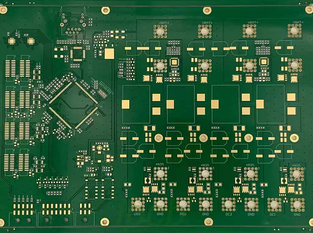
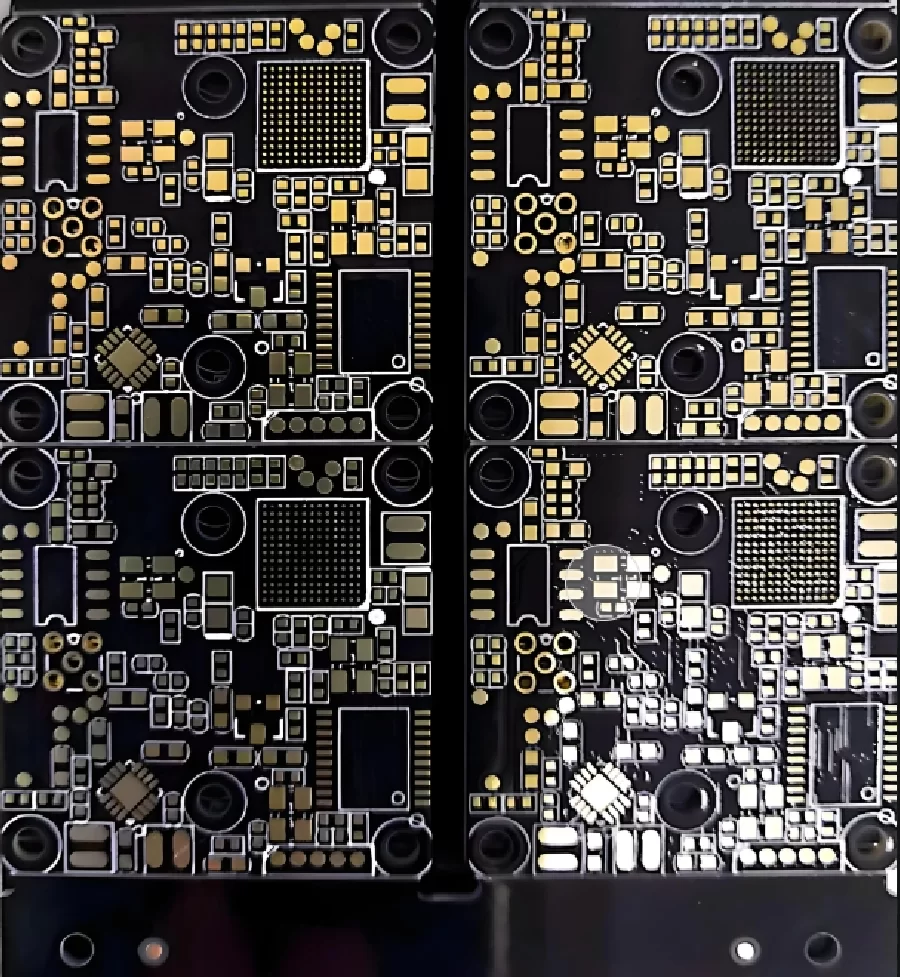
Placing vias directly in PCB pads has long been a controversial design practice in hardware layout and routing. Engineers who are new to PCB layout often wonder why, despite the widespread adoption of resin via plugging, most design guidelines still discourage placing vias directly in conventional signal pads. To understand this issue, it is necessary to consider SMT reflow soldering defects and PCB manufacturing costs while distinguishing between scenarios where via-in-pad should generally be avoided and specific applications where it is technically feasible.
In the early days of PCB manufacturing, most boards supported only conventional through-hole vias, while mature resin via plugging processes were not yet widely available. Industry guidelines generally prohibited placing vias directly in BGA pads. The most immediate risk was solder paste leakage. After stencil printing, solder paste could easily flow downward through the via barrel, leaving insufficient solder on the pad surface.
During reflow soldering, the BGA solder ball could then fail to form a reliable solder joint, resulting in insufficient solder joints, open solder joints, and solder joint separation. Due to these process limitations, the standard practice was to route a short trace out from the pad and place the via in an open area outside the pad to complete the fanout.
Today, resin via plugging can seal the via barrel and fundamentally reduce the risk of solder paste leakage. However, this does not mean that vias can be freely placed in any pad. Even when solder leakage is eliminated, long-term reliability concerns remain. Under thermal cycling, microscopic gaps can develop at the interfaces between the pad, plugging resin, and copper plating on the via wall.
Moisture can gradually penetrate these interfaces and accelerate solder joint corrosion. In addition, resin via plugging and board-surface planarization introduce additional manufacturing processes, directly increasing PCB fabrication costs. Considering yield, cost, and surface uniformity, engineers generally avoid placing vias directly in signal pads unless routing space is extremely limited.
In addition to BGA soldering concerns, small chip components are also susceptible to tombstoning. Miniature passive components such as 0201 and 0402 resistors and capacitors are particularly prone to tombstoning during reflow soldering. Tombstoning occurs when one end of a component lifts away from the solder pad during reflow, leaving only one side electrically connected and causing the component to stand upright like a tombstone. The fundamental failure mechanism is an imbalance in the surface tension of the molten solder at the two ends of the component.
If a via is placed on one pad of a surface-mount component or near the edge of the pad, the thermal conductivity and copper area of the two pads become unbalanced. The pad containing the via may heat up faster, causing the solder paste to melt earlier and its surface tension to decrease rapidly. The solder on the opposite pad melts later and retains a stronger surface-tension force, pulling the component upward and causing it to rotate.
The smaller and lighter the component, the more pronounced the effect of this surface-tension imbalance becomes, which can significantly increase the defect rate during mass production. This is a key reason why PCB design rules for small passive components generally impose strict restrictions on placing vias close to solder pads.
However, placing vias directly in PCB pads is not universally prohibited. Depending on the package characteristics and PCB manufacturing process, there are two applications that are widely accepted in the industry and frequently used in practical engineering.
The first is the use of blind and buried vias with ultra-fine-pitch BGA packages. When the BGA ball pitch is 0.5 mm or smaller, conventional trace fanout often leaves insufficient routing space, while conventional through-hole vias can easily interfere with adjacent traces. In such cases, blind and buried vias can provide an effective solution.
A blind via connects an outer-layer trace to a designated internal layer of the PCB without passing through the entire board. A buried via is used only to interconnect internal PCB layers and cannot be observed from the finished board surface. Neither type of via creates the same through-hole path that allows solder paste to leak into the board. They are therefore commonly used for high-density via-in-pad structures, including Plated Over Filled Via (POFV) designs.
However, blind and buried via technology requires processes such as laser drilling and sequential lamination, which can significantly increase PCB manufacturing costs. It is therefore generally suitable for high-end, high-density mainboards rather than conventional control boards or power boards, where such technology may not be economically justified.
The second application is the use of thermal vias in the exposed thermal pad beneath power devices. Datasheets for power ICs and power MOSFETs often recommend placing an array of thermal vias in the large exposed thermal or ground pad at the center of the package. These thermal vias are not subject to the same design restrictions as conventional signal pads because the thermal pad is not responsible for signal-pin soldering. Its primary function is to transfer heat generated by the device into the PCB and improve thermal dissipation.
During reflow soldering, the entire thermal pad is covered with solder, so there is no asymmetric solder surface-tension condition between two separate pads that could cause tombstoning. Through-hole thermal vias can connect the thermal pad to large copper planes on internal layers, further strengthening the thermal conduction path. This is a well-established technique in power electronics design. The key considerations are appropriate via diameter and pitch, together with sufficient solder coverage on the thermal pad.

Practical PCB Design Guidelines
For conventional industrial control boards and consumer electronics PCBs, passive components and standard BGA packages should generally use fanout routing with vias placed outside the pads. This approach provides a better balance among soldering yield, manufacturing cost, and long-term reliability.
For ultra-fine-pitch BGA packages with a pitch of 0.5 mm or smaller, evaluate the project budget before deciding whether to adopt blind and buried vias or POFV technology. At the same time, confirm the resin via plugging and board-surface planarization requirements with the PCB manufacturer.
For thermal vias beneath power devices, strictly follow the recommendations in the device datasheet when determining via placement, diameter, and pitch. The design should balance thermal performance with adequate solder coverage during SMT assembly.
When preparing PCB fabrication specifications, clearly distinguish between the two design rules: conventional through-hole vias should generally be prohibited directly in signal pads, while thermal vias are permitted in exposed thermal pads where required for thermal management. This helps reduce misunderstandings with the PCB manufacturer and minimizes potential risks during mass production.
Via-in-pad is a design solution with specific application constraints rather than a universally preferred PCB layout method. For most conventional circuits, trace fanout with vias placed outside the pcb pads remains the preferred approach. Only when high-density routing creates a significant space constraint or high-power devices require enhanced thermal management should an appropriate via structure be selected, with the final decision based on manufacturing cost, process capability, and soldering reliability.