In modern surface mount and high-reliability electronic packaging, when systems face extreme temperatures of hundreds of degrees Celsius, high voltage isolation of thousands of volts, severe mechanical vibration, and the heat dissipation challenges posed by extremely high power density, ordinary organic copper-clad laminates (ECC) and even metal-based copper-clad laminates (MCPCBs) are highly susceptible to substrate carbonization, interlayer delamination, and insulation breakdown.
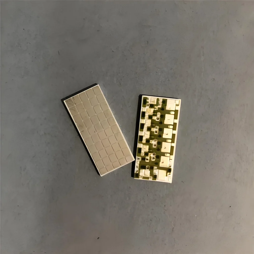
Thick film ceramic substrates, with their excellent mechanical rigidity, superior thermal conductivity, high volume resistivity, and excellent heat aging resistance, have become a key physical carrier for power semiconductors, automotive electronics (such as engine control units and brake system sensors), high-power LEDs, aerospace microelectronics, and thick-film hybrid integrated circuits (HMICs).
The essence of thick-film ceramic substrates is that, through precise paste printing and high-temperature sintering processes, functional pastes are transformed into metal conductor networks, precision resistors, or insulating dielectric layers firmly attached to the ceramic substrate on the surface of a high-purity inorganic ceramic sheet. A thorough analysis of the microstructure of thick-film ceramic substrates, the physicochemical reactions at the high-temperature sintering interface, precision printing manufacturing processes, thermal resistance and stress matching mechanisms, and typical engineering failure modes is of decisive engineering value for designing highly stable, long-life electronic systems for extreme environments.
Microstructure and Thermophysical Properties of Ceramic Substrates
Thick-film technology places extremely high demands on the physical and chemical stability of ceramic substrates. During high-temperature sintering, the substrate must maintain dimensional stability and not deform, and must form a good interfacial bond with the glass phase or oxides in the thick-film slurry. The most commonly used substrate is 96% alumina (Al2O3) ceramic by mass. 96% alumina ceramic is not a single-crystal structure, but a polycrystalline composite material composed of micron-sized alumina grains and silicate glass phase sintering aids distributed at the grain boundaries. The introduction of sintering aids lowers the sintering temperature of the ceramic, giving the substrate excellent physical rigidity and economy. Its thermal conductivity is typically between 24 and 28 W/m·K, more than 80 times that of traditional FR-4 substrates. Simultaneously, its coefficient of thermal expansion (COP) of 6.5 to 7.5 is highly compatible with semiconductor silicon and silicon carbide chips, significantly reducing interfacial shear stress under thermal cycling. In scenarios with extremely demanding heat dissipation requirements, aluminum nitride (AlN) ceramics have become an important upgrade option. Aluminum nitride boasts a thermal conductivity of 170 to 200 W/m·K, more than 7 times that of alumina. However, aluminum nitride is a non-oxide ceramic, and its surface chemistry is incompatible with the thick-film pastes traditionally used for alumina. Before printing the thick-film paste, the aluminum nitride substrate must undergo surface pre-oxidation treatment in a high-temperature air atmosphere to artificially generate a protective film of silicon dioxide or silicate oxide tens of nanometers to several micrometers thick on its surface, ensuring that the subsequent thick-film paste can be wetted and firmly anchored during sintering.
Composition of Thick Film Functional Pastes and High-Temperature Sintering Interface Chemistry
The core manufacturing process of thick film ceramic substrates lies in the preparation and sintering of functional pastes. Thick film pastes are not ordinary inks, but rather a fluid composed of a mixture of organic and inorganic components.
Thick film pastes typically consist of three parts:
- Functional Phase: This determines the electrical properties after sintering. For conductor pastes, the functional phase is usually noble metal powders (such as gold, silver, palladium-silver alloys, platinum, or copper); for resistive pastes, the functional phase is usually a metal oxide with semiconductor properties (such as ruthenium dioxide RuO2 or ruthenates); for dielectric pastes, the functional phase is highly insulating glass powder or low dielectric constant ceramic powder.
- Binder Phase: This determines the adhesion between the film layer and the ceramic substrate. The binder phase is mainly divided into glass-bonded and oxide-bonded/reactive-bonded phases. The glass phase is typically borosilicate glass powder, which melts and wets the ceramic surface during sintering. The oxide phase utilizes molten oxides such as copper oxide and cadmium oxide to react with alumina ceramics in a solid-state reaction, forming a spinel crystalline layer.
- The organic vehicle is composed of polymer resins (such as ethyl cellulose) and high-boiling-point organic solvents (such as terpineol), imparting suitable viscosity and thixotropy to the slurry, ensuring clear and non-sagging patterns during screen printing.
The most classic sintering process for interfacial reaction physical thick-film substrates using air sintering at 50°C is a continuous tunnel furnace sintering at a peak temperature of approximately 850°C. The entire sintering process is physically and chemically divided into three stages: the first stage is the organic matter volatilization and decomposition zone (100 to 500°C): the organic solvent evaporates rapidly, and the resin polymer undergoes thermal re-oxidation decomposition in the air atmosphere, converting into gases that are expelled. Good exhaust flow must be maintained within the furnace to prevent carbon residue from degrading the insulation performance of the film. The second stage is the high-temperature melting and interfacial reaction zone (750 to 850 degrees Celsius): the glass powder particles in the slurry begin to soften and melt into a liquid phase. Under capillary force, the liquid glass fills the gaps between the metal particles, while simultaneously strongly wetting the alumina ceramic surface. At the peak temperature, the molten glass diffuses and dissolves with the silicate microphase at the alumina grain boundaries, or the active oxides react with alumina to form a microscopic coherent interface. The third stage is the crystallization and cooling solidification zone (850 to room temperature): as the temperature decreases, the liquid glass re-solidifies, firmly encapsulating and “anchoring” the metal particles to the ceramic substrate surface, forming a dense, continuous conductive or resistive film layer.
Screen printing and high-precision patterning processes: The preparation of thick film patterns relies on a highly precise screen printing process.
During printing, the ceramic substrate is fixed on a vacuum adsorption stage, and a high-mesh stainless steel wire mesh (typically 200 to 325 mesh) is stretched taut on the frame. A screen is coated with photoresist and developed to reveal the desired circuit pattern. A squeegee moves across the screen at a specific angle, pressure, and speed, causing the screen to undergo minute elastic deformation and contact the ceramic surface (this distance is called the snap-off distance). This forces the paste through the mesh openings onto the ceramic substrate.
To obtain high-precision thick-film circuitry, rheological control during the printing process is crucial. The paste must possess excellent thixotropy: under the shearing force of the squeegee, the paste viscosity drops sharply, allowing it to flow smoothly through the mesh openings; when the squeegee is removed, the shearing force disappears, and the paste viscosity must rapidly recover within seconds to prevent the pattern from spreading across the ceramic surface, causing linewidth distortion or short circuits.
The printed wet film needs to be dried in an oven at 125 to 150 degrees Celsius for 10 to 15 minutes to remove volatile organic solvents, transforming it into a dry film with sufficient mechanical strength. It is then sent to a tunnel furnace for high-temperature sintering. For fabricating multilayer thick-film circuits or cross-wiring, a repeated “printing-drying-sintering” cycle is required, or a multi-printing-drying-sintering overlay process must be employed.
Laser Trimming and Precision Resistor Manufacturing
A major irreplaceable advantage of thick-film ceramic substrates is their ability to directly integrate high-precision thick-film resistors onto the substrate.
However, due to screen mesh fluctuations, uneven printing thickness, and slight temperature drift in the sintering furnace, the initial resistance tolerance of sintered thick-film resistors is typically around 10% to 20%, which cannot meet the requirements of precision circuits. To obtain high-precision resistance values, a high-energy Q-switched pulsed laser (such as an Nd:YAG laser) must be used to perform laser trimming on the sintered thick-film resistors.
The physical process of laser resistance trimming is as follows: A laser beam is focused on the surface of a thick-film resistor, instantly generating temperatures of thousands of degrees Celsius. This vaporizes and ablates part of the resistive film, cutting a micrometer-sized slit (called a trimming notch). The introduction of the notch alters the current flow distribution within the resistor, reducing the effective conductive cross-sectional area, thus causing the resistance value to increase monotonically. Simultaneously with laser cutting, a measurement system monitors the resistance value across the resistor in real time. When the resistance reaches the preset target accuracy (tolerance can reach 0.1% or even higher), the laser beam instantly stops cutting.
Common laser notch topologies include single-blade cuts (I-Cut), double-blade cuts (L-Cut), and serpentine cuts. The L-Cut process first cuts perpendicular to the current direction to quickly approach the target resistance value, then bends 90 degrees to fine-tune along the current direction. This ensures extremely high trimming accuracy while avoiding long-term resistance drift caused by concentrated electric field at the notch tip.
Thermal Management and Electrical Insulation Physical Properties
In power electronic packaging, thick-film ceramic substrates play a dual role as heat dissipation paths and electrical isolation barriers. Because the ceramic substrate itself is an excellent insulator, its volume resistivity is typically greater than 10^14 ohm-cm, and its dielectric breakdown strength is as high as 15 to 20 kV per millimeter. This means that high-voltage isolation of several kilovolts can be easily achieved on a ceramic sheet only 0.635 mm thick, without the electrical treeing aging and breakdown that occurs under long-term high voltage conditions like traditional organic insulating layers. In terms of thermal conduction, thick-film ceramic substrates rapidly conduct heat generated by the chip’s heat source to the bottom surface along the thickness direction. Although the conductor layer thickness of thick-film sintering (typically around 10 to 20 micrometers) is much thinner than the thick copper layer of direct copper clad laminate (DBC), making it difficult to provide a strong lateral heat spreading effect, thick-film processes can create extremely low thermal resistance heat dissipation channels by printing a high thermal conductivity metal underlayer over a large area on the back of the ceramic substrate or by soldering it to a metal heat sink. For scenarios requiring the handling of tens of amperes of current, traditional single-printed thick-film conductors generate significant resistive heat due to their thin film layer.
In such cases, heavy-print thick film or thick-film copper/gold paste processes can be used to increase the metal conductor thickness to 50 micrometers or even over 100 micrometers through multiple printing and sintering processes, significantly reducing circuit resistance and current-carrying temperature rise.
Assembly, soldering, bonding performance, and engineering failure analysis
After sintering and resistance repair, thick-film ceramic substrates need to be assembled with various passive devices, semiconductor chips, and housings.
Surface Metallization Plating and Bonding Applicability The metal material of the thick-film conductor layer directly determines the subsequent assembly process:
Palladium/Silver (Ag/Pd) or Platinum/Silver (Ag/Pt) Conductors: These are the most cost-effective and widely used thick-film conductors. The addition of palladium or platinum greatly suppresses the “silver-eating” phenomenon (silver dissolving into molten solder) during high-temperature soldering, while also preventing silver atom electrochemical migration under humid bias conditions. Suitable for traditional tin-lead or lead-free solder paste SMT surface mount soldering.
Pure Gold (Au) Conductors: Primarily used in microwave and military circuits requiring extremely high reliability. Gold conductor layers do not oxidize, have extremely low RF loss, and are perfectly suited for gold wire bonding (thermo-pressing/ultrasonic bonding), enabling high-density interconnection between the chip and the substrate.
Pure Copper (Cu) Conductors: Due to the rapid and severe oxidation of copper in high-temperature air, thick-film copper slurries must be sintered at 900°C in a tunnel furnace under a pure nitrogen protective atmosphere. Copper conductors possess excellent conductivity and resistance to silver erosion, making them ideal for soldering high-power components and aluminum wire bonding.
Common Engineering Failure Modes and Prevention Mechanisms: Failures of thick-film ceramic substrates throughout their lifecycle are typically closely related to mechanical stress, environmental corrosion, and thermal shock:
Failure 1: Silver Migration Leading to Interlayer or Line-to-Line Short Circuits
On thick-film substrates containing pure silver or low-palladium silver conductors, if the surface is not coated with a moisture-proof dielectric protective layer and is exposed to a humid environment for a long period, under DC bias, silver atoms will oxidize and dissolve at the anode to form silver ions. Driven by an electric field, these silver ions migrate through the moisture film to the cathode, where they are reduced and precipitated as dendritic metallic silver. As the dendritic silver crystals continue to grow and extend to the anode, catastrophic insulation breakdown short circuits can occur between adjacent traces.
Engineering preventative measures include: using palladium-silver paste with a high palladium content (typically greater than 15% to 20%); and printing and sintering a dense layer of low-melting-point glass overglaze over the sensitive silver conductor lines to completely isolate the conductor from external moisture.
Failure 2: Interfacial Delamination under Thermal Cycling The adhesion between the thick-film conductor layer and the ceramic substrate depends on the micro-interlocking of the sintered glass phase. When the device undergoes severe repeated thermal cycling (e.g., from -55°C to 150°C), due to the mismatch in thermal expansion coefficients among the metal conductor layer, the glass phase, and the ceramic substrate, enormous thermal shear stress accumulates at the interface. After multiple cycles, the micro-glass anchoring structure fatigues and fractures, causing the metal conductor to peel off completely from the ceramic surface.
Engineering preventative measures include: strictly controlling the peak sintering temperature and holding time to ensure complete wetting of the glass phase and the formation of an interface reaction layer of optimal thickness; and implementing stress-relieving design for the solder terminals to avoid direct normal pull-out forces at the solder joints.
Failure 3: Substrate Cracking Alumina ceramics are brittle materials with high hardness but low fracture toughness. When mounting thick-film ceramic substrates onto housings or heat sinks, uneven mounting surfaces, excessive screw tightening torque, or uneven stress can generate significant bending stress within the ceramic. Once the local tensile stress exceeds the ceramic’s bending strength, the substrate will experience instantaneous brittle fracture.
Engineering preventative measures include: ensuring extremely high flatness of the heat dissipation mounting surface; using flexible thermal interface materials (TIM) or thermally conductive adhesives for bonding and leveling; leaving sufficient buffer zones around mechanical mounting holes and strictly prohibiting screws from directly pressing against exposed ceramic edges.
Thick Film Ceramic Substrate Engineering Design Checklist
To ensure smooth operation of thick film ceramic substrates from circuit design and paste selection to manufacturing, engineers should check the following guidelines item by item before issuing manufacturing drawings:
Substrate Specifications and Dimensions Selection: Confirm the substrate material (e.g., 96% alumina or aluminum nitride), substrate thickness (commonly 0.25mm, 0.38mm, 0.635mm, 1.0mm), and dimensional tolerances; confirm the margin for laser scribing/grooving boundaries.
Line Width, Spacing, and Screen Aperture Design: For standard thick film printing, line width and spacing should be controlled above 125 micrometers (5 mil); for fine circuit designs, the feasibility of direct polycarbonate (DPC) processing needs to be evaluated; large-area grounding copper pours require a gridded aperture design to prevent substrate warping due to excessive stress during sintering.
Slurry Matching and Sintering Sequence: The conductor slurry type (e.g., Ag/Pd, Au, Cu) must be clearly specified according to welding and bonding requirements. If multi-layer printing is involved, the sintering sequence (Co-firing or Sequential Firing) of the dielectric layer, conductor layer, and resistor layer must be clearly indicated.
Resistor Design and Laser Resistance Repair: The aspect ratio (Square Count) of the thick-film resistor must be accurately calculated based on the sheet resistance slurry specifications. A minimum clearance of 0.5 mm must be left around the resistor to prevent high-energy pulse damage to adjacent conductors or components during laser resistance repair.
Overglaze Coverage: For all silver-based conductors exposed to air and under bias, an overglaze glass pattern must be designed. The edge of the overglaze must extend at least 0.2 mm beyond the conductor edge to completely block moisture migration paths.