A custom PCBA is a printed circuit board assembly manufactured according to the specific electrical, mechanical, component, assembly, and testing requirements of a particular electronic product. Unlike a bare PCB, which provides only the physical circuit structure, a PCBA includes the electronic components mounted and soldered onto the board. The word “custom” is important because the finished assembly is built around a specific product design rather than a standard, off-the-shelf board.
In practical manufacturing, custom PCBA can involve much more than placing components onto a PCB. Depending on the project, it may include PCB fabrication, component sourcing, SMT and through-hole assembly, programming, inspection, electrical testing, functional testing, and preparation for integration into the final product. The exact combination depends on what the board is designed to do and how it will be produced.
This makes custom PCBA particularly relevant to companies developing their own electronic hardware. The same manufacturing approach does not necessarily work for a simple controller board, a high-speed communication device, an industrial control system, or a compact consumer product. Each design introduces different requirements that have to be considered before production begins.
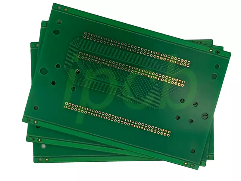
The distinction between PCB and PCBA is straightforward but important. A PCB is the fabricated circuit board itself, containing copper traces, pads, vias, insulating materials, and other structures needed to create the electrical connections. A PCBA is the assembled version after components have been mounted and soldered onto the board.
A custom PCBA takes this one step further because the assembly process is adapted to a particular product design. The component package types, component locations, soldering process, PCB construction, inspection requirements, programming requirements, and functional tests are determined by the project.
For example, one product may use predominantly SMT components and require automated optical inspection after reflow. Another may combine SMT devices with through-hole connectors that require an additional soldering process. A board with BGA components may require X-ray inspection because some solder joints are hidden beneath the package. A programmable control board may also need firmware loaded before it can undergo functional testing.
Consequently, there is no single manufacturing process that can be described as the standard custom PCBA process for every product. The manufacturing route has to follow the design.
Why Custom PCBA Requires Engineering Review Before Production
A common mistake in PCBA procurement is to treat the manufacturing stage as something that begins after the PCB design has already been completed. In reality, many production problems can be identified before components are purchased or the first board is assembled.
A DFM, or Design for Manufacturability, review examines whether the design can be manufactured consistently using the intended PCB fabrication and assembly processes. It can identify issues involving component spacing, pad design, PCB tolerances, component orientation, soldering access, board construction, and other manufacturing constraints.
This review becomes particularly important when the design is new or when a prototype is being transferred into larger-scale production. A circuit may work correctly on an engineering prototype while still having assembly characteristics that make it difficult to manufacture repeatedly.
The purpose of DFM is therefore not simply to find obvious design errors. It is to reduce the gap between a PCB that can be assembled once and a PCBA that can be manufactured reliably over many production cycles.
Before a custom PCBA manufacturer can determine the appropriate production process, the project documentation needs to describe the board accurately.
Gerber files normally define the PCB fabrication information, while the BOM identifies the components required for assembly. Pick-and-place or centroid data provides component placement information, and assembly drawings can provide additional information about component orientation, polarity, special requirements, or mechanical details. Test procedures and acceptance criteria may also be necessary when functional testing is part of the project.
The exact file package varies between projects, but manufacturers commonly request Gerber files, BOMs, Pick-and-Place files, assembly drawings, schematics, and testing requirements before beginning a manufacturing review.
The quality of this information directly affects the efficiency of the project. An incomplete BOM, inconsistent reference designators, missing component specifications, or unclear assembly instructions can create delays long before the first solder joint is made.
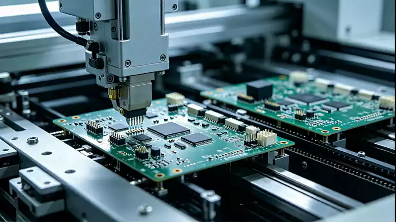
Component Sourcing Can Have a Major Effect on Custom PCBA
For many custom PCBA projects, component procurement is one of the most difficult parts of production.
The BOM may contain hundreds of individual components, ranging from common passive devices to processors, connectors, sensors, memory devices, power components, and other specialized parts. Their availability, package type, manufacturer part number, lifecycle status, and acceptable alternatives all need to be considered.
A component that is available during prototype development may not necessarily remain readily available when the product enters volume production. Conversely, selecting a substitute without proper engineering approval can change electrical or mechanical characteristics and create new problems.
For this reason, component sourcing should not be separated completely from the PCBA manufacturing process. BOM validation and approved alternative management can help identify potential supply risks before they affect the production schedule.
In projects where the customer supplies the components, the manufacturing process also needs to account for incoming material inspection, quantity verification, packaging requirements, and component handling.
SMT and Through-Hole Assembly Serve Different Requirements
Surface Mount Technology is the dominant assembly method for many modern PCBAs because it allows components to be placed directly onto the PCB surface and supports high component density and automated production.
The process generally involves solder paste printing, component placement, and reflow soldering. The quality of the solder paste deposits and component placement has a direct influence on the final assembly quality.
Through-hole technology remains important where components or connectors require mechanical reinforcement, larger terminals, or a particular electrical or mechanical structure. Some custom PCBAs therefore use a combination of SMT and through-hole components rather than relying exclusively on one technology.
The assembly process needs to account for the complete component mix. A board containing fine-pitch SMT devices, large thermal-mass components, and through-hole connectors may require a more carefully controlled production sequence than a simple SMT assembly.
Inspection and Testing Should Match the Product
Inspection and testing are not interchangeable.
Automated Optical Inspection can examine visible solder joints and component placement, while X-ray inspection can provide visibility into certain hidden solder connections, such as those associated with BGA packages. Electrical tests can check circuit continuity or other electrical characteristics, while functional testing verifies whether the assembled board actually performs its intended function.
A custom PCBA may require one or several of these approaches depending on the product.
For example, a relatively simple board may require visual inspection and AOI as its primary production controls. A complex digital board may require additional electrical or functional testing. A board containing BGA devices may benefit from X-ray inspection as part of the quality-control strategy.
The important point is that the test plan should be developed around the product’s actual failure risks rather than adding every possible inspection method regardless of its value.
What Determines the Cost of Custom PCBA
The price of a custom PCBA is influenced by much more than the size of the PCB.
The BOM can be one of the largest cost factors because the number, type, availability, and price of components directly affect the finished assembly. PCB construction also matters, particularly when the board requires many layers, special materials, tight manufacturing tolerances, advanced via structures, or specific surface finishes.
Assembly complexity contributes additional cost. Fine-pitch components, BGA packages, mixed SMT and through-hole technology, unusual component sizes, special soldering processes, and additional inspection can all change the production requirements.
Testing is another factor. A board requiring only basic inspection has a different manufacturing cost from one requiring dedicated ICT fixtures, functional test equipment, programming, burn-in, or other specialized procedures.
Production quantity also changes the economics. A prototype may carry higher unit costs because engineering preparation, setup, component purchasing, and testing are distributed across a small number of boards. Larger production quantities can distribute these fixed costs across more units, although the actual economics depend on the product and manufacturing process.
This is why comparing custom PCBA quotations based solely on unit price can be misleading. Two quotations may appear similar while covering different PCB specifications, component sourcing arrangements, inspection levels, testing requirements, or production assumptions.
Design for Testing Becomes Important as Complexity Increases
Design for Test, or DFT, is closely related to DFM but focuses on how effectively the finished PCBA can be inspected and tested.
As boards become denser, some circuit nodes become difficult to access physically. Test points, programming interfaces, diagnostic connections, and functional test access therefore need to be considered during PCB design.
A board that is easy to manufacture but difficult to test can create problems during production. Conversely, incorporating appropriate test access into the design can make fault detection faster and improve production consistency.
For custom PCBA, DFM and DFT should ideally be considered before the first prototype rather than treated as corrections after production problems appear.
What a Manufacturer Needs to Know Before Quoting a Custom PCBA
A useful quotation requires enough information to understand what is actually being manufactured.
At minimum, the manufacturer normally needs the PCB design data, BOM, required quantity, and assembly requirements. For more complex products, information about testing, programming, special components, mechanical requirements, target delivery schedule, and production location may also be important.
The quantity should be stated clearly because prototype, low-volume, and mass-production requirements can involve different manufacturing assumptions. Component sourcing should also be clarified because customer-supplied components and turnkey sourcing create different procurement responsibilities.
When the documentation is incomplete, an initial engineering review can often identify what information is missing before a final quotation is prepared.
How to Approach a Custom PCBA Project
The most reliable approach is to treat custom PCBA as an engineering and manufacturing process rather than simply an assembly purchase.
The project begins with the electronic design and manufacturing documentation. The manufacturer then reviews the PCB, BOM, assembly requirements, component availability, and testing strategy. DFM and DFT considerations can be addressed before production, followed by prototype assembly and validation.
Once the prototype has demonstrated that the design and manufacturing process are viable, the project can move toward pilot production and eventually volume manufacturing. At each stage, production data and engineering feedback can be used to identify issues before they become more expensive to correct.
This approach is particularly useful for products that are expected to remain in production for an extended period. The goal is not simply to produce the first batch successfully, but to establish a manufacturing process that can remain stable as production continues.
Custom PCBA is the process of turning a product-specific PCB design into a functional electronic assembly through component sourcing, assembly, soldering, inspection, testing, and other manufacturing operations required by the project.