How Does a Circuit Board Work?A circuit board works by providing fixed electrical paths between electronic components. These paths are formed mainly by copper traces on an insulating substrate, allowing power and electrical signals to move between components in a controlled way. The board also provides the mechanical structure needed to hold those components in their intended positions.
When a device is powered on, electricity enters the circuit board through a connector, battery connection, or another power source. The PCB then distributes that electrical power to the components through copper traces, planes, vias, and other conductive structures. Components such as resistors, capacitors, diodes, transistors, and integrated circuits modify, control, store, or process the electrical energy and signals according to the circuit design.
The circuit board itself does not normally perform the logic of the electronic system. Instead, it provides the physical electrical connections that allow the components to work together as the circuit intended by the designer.
How a Circuit Board Creates Electrical Connections
A PCB starts with an electrically insulating substrate and one or more layers of copper. The copper is patterned into traces, pads, planes, and other conductive features. These structures replace the individual wires that would otherwise be needed to connect electronic components.
A copper trace functions much like a fixed wire. It connects one point of the circuit to another and provides a path for current or electrical signals. Pads provide the locations where component terminals are attached, while vias can establish electrical connections between different copper layers in a multilayer PCB.
This arrangement allows a complex circuit to be physically organized on a relatively small board. Instead of manually wiring every resistor, capacitor, IC, and connector, the PCB permanently defines the required connections through its copper pattern.
The result is a repeatable electrical network that can be manufactured and assembled consistently.
What Happens When Power Is Applied
Consider a simple electronic circuit containing a power source, resistor, LED, and ground connection.
When the power source is connected, a voltage difference is established across the circuit. Current can then flow through the conductive path created by the PCB traces and the connected components.
The resistor limits the current reaching the LED, while the LED converts part of the electrical energy into light. The current then returns through the appropriate circuit path to the power source.
The PCB does not decide that the LED should illuminate. The component arrangement and circuit design determine that behavior. The PCB simply provides the conductive paths that allow the intended electrical relationships to exist.
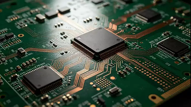
In more complicated electronics, the same principle applies even though the number of components and connections may be much larger. A computer motherboard, for example, can contain processors, memory devices, power circuits, connectors, storage interfaces, and many other components connected through an intricate multilayer PCB.
How Components Work With the PCB
The electronic components mounted on a circuit board perform different electrical functions.
Resistors can limit current or establish voltage relationships. Capacitors can store electrical charge and are widely used for filtering and power decoupling. Diodes control current direction or perform functions such as rectification and protection. Transistors can switch or amplify electrical signals. Integrated circuits contain much more complex electronic functions within a single package.
The PCB connects these components according to the schematic and layout created during the design process.
For example, a capacitor may need to be connected between a power rail and ground. The PCB provides copper paths from the capacitor’s pads to those electrical nodes. A microcontroller may have dozens or hundreds of connections, with individual traces or planes carrying power, ground, clocks, data, and control signals.
This is why PCB layout is more than simply deciding where components should be placed. The physical routing determines how the electrical circuit is implemented.
The Role of Copper Traces
Copper traces are one of the most important parts of a circuit board because they provide the conductive paths between components.
In a simple PCB, a trace may connect two components over a short distance. In a multilayer board, traces can travel across different layers and connect through vias. Power and ground may also be distributed through larger copper areas rather than narrow traces.
Trace width and geometry depend on the electrical requirements of the circuit. A power path carrying significant current may require more copper than a low-current signal connection. High-speed signals can have additional requirements involving impedance, spacing, return paths, and layer structure.
Therefore, the copper pattern is not arbitrary. It is the physical implementation of the electrical design.
How Vias Connect Different PCB Layers
A multilayer circuit board contains several copper layers separated by insulating material. Without some method of connecting those layers, each layer would essentially function as a separate circuit.
Vias solve this problem by creating conductive connections between selected PCB layers. A plated through-hole can connect multiple layers through the board, while other via structures can connect only specific layers depending on the PCB construction.
For example, a signal may begin on the top layer, pass through a via, continue along an internal layer, and then transition to another layer through another via.
This makes it possible to route thousands of electrical connections through a compact multilayer board.
As PCB density increases, via structure becomes increasingly important. The choice of through vias, blind vias, buried vias, or microvias can influence routing density, electrical performance, manufacturing complexity, and cost.
How Surface-Mount and Through-Hole Components Connect
Electronic components can be attached to a PCB using different assembly technologies.
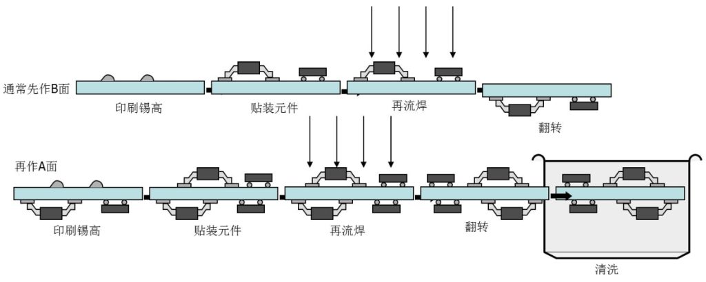
With surface-mount technology (SMT), components are soldered directly onto pads on the surface of the PCB. This allows relatively small components and high component density.
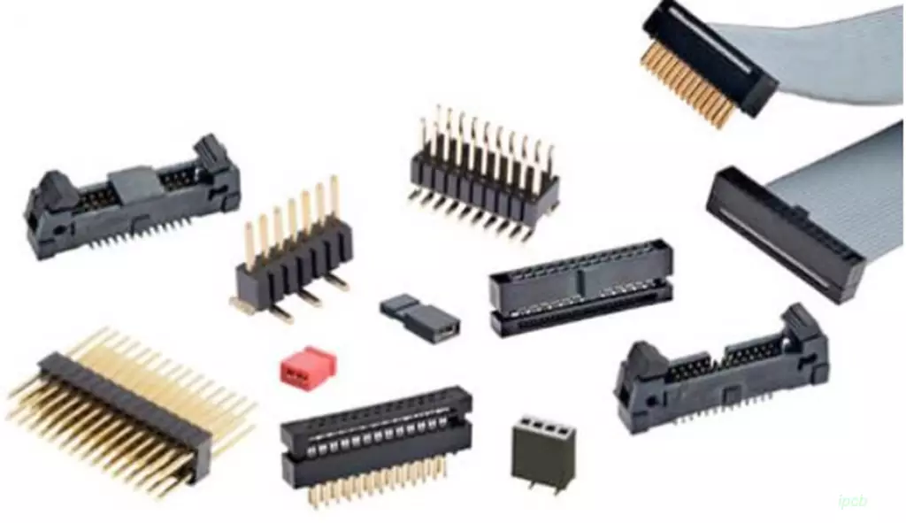
With through-hole technology (THT), component leads pass through holes in the PCB and are soldered to conductive areas associated with those holes. Through-hole construction can provide strong mechanical connections and remains useful for certain connectors and larger components.
Many modern circuit boards combine both methods. A PCB might use SMT for integrated circuits, resistors, capacitors, and other compact components while using through-hole mounting for mechanically demanding connectors or other components.
The solder joint provides both the electrical connection and, depending on the assembly method and component, mechanical attachment.
How Multilayer Circuit Boards Work
A multilayer PCB works according to the same basic electrical principle as a simple single-layer board, but it provides additional copper layers and insulation to accommodate more complex circuits.
Internal layers can be used for signal routing, power distribution, and ground planes. These layers are separated by dielectric materials, while vias provide connections between selected conductive layers.
Using internal power and ground planes can also provide advantages for high-speed designs because the reference plane helps establish a predictable electrical environment for signal traces. Four-layer and higher-layer PCBs are therefore common when the routing density and electrical requirements exceed what a simple two-layer board can accommodate.
The number of layers is not simply a measure of board quality. A designer selects the layer count according to routing requirements, signal integrity, power distribution, mechanical constraints, manufacturing capability, and cost.
Why Circuit Board Layout Affects Electrical Performance
A circuit can have the correct schematic and still encounter problems if the PCB layout is poorly designed.
At low frequencies and simple applications, the physical arrangement of traces may have relatively little effect on circuit behavior. As signal speeds and frequencies increase, however, the physical dimensions of the PCB become increasingly important.
Trace length, width, spacing, dielectric thickness, copper geometry, vias, and reference planes can influence signal integrity. Poor routing can contribute to reflection, crosstalk, electromagnetic interference, and signal loss.
Power distribution also needs careful attention. A processor or other high-performance device may experience rapidly changing current demands, so the PCB must provide an appropriate low-impedance path between the power delivery network and the load.
For this reason, modern PCB design often considers signal integrity and power integrity alongside traditional circuit connectivity.
How the PCB Becomes a Working Circuit
The circuit board only becomes a functional electronic assembly after the designed components are installed and electrically connected.
The process begins with a schematic that defines the intended electrical relationships. PCB design software then converts those relationships into a physical layout containing component footprints, copper traces, pads, vias, planes, and other board features.
The PCB is fabricated according to this layout. Copper patterns are formed on the required layers, the layers are combined for multilayer boards, holes and vias are created, and protective finishes such as solder mask are applied. The resulting bare PCB contains the physical electrical network but does not yet contain the active and passive components required for the final circuit.
During assembly, components are mounted and soldered onto the board. Once the appropriate components are connected, the PCB becomes a complete PCBA capable of performing the intended electronic function.
Testing can then verify whether the assembled circuit operates as expected.
Why Circuit Boards Are Used Instead of Individual Wires
Before PCBs became widely used, electronic circuits could be assembled using point-to-point wiring. This approach becomes increasingly difficult as the number of components grows.
A PCB replaces many individual wires with a precisely manufactured conductive pattern. This reduces wiring complexity and allows components to be positioned in a compact and repeatable arrangement. SparkFun describes one of the fundamental functions of a PCB as routing signals and power between physical devices.
The approach also makes large-scale production practical. Once a PCB design has been finalized, the same copper pattern can be reproduced across many boards, providing consistent electrical connections from one unit to the next.
This repeatability is one of the main reasons PCBs are fundamental to modern electronics.
How Circuit Boards Handle More Complex Electronics
The basic principle remains the same whether the board contains a few components or thousands of them.
A simple control circuit may use a small two-layer PCB with a microcontroller, several sensors, resistors, capacitors, and connectors. A high-performance computing board may contain many PCB layers, high-density packages, power delivery circuits, high-speed interfaces, and complex thermal structures.
The difference lies in the number and characteristics of the electrical connections.
As the circuit becomes more complex, designers need greater control over the physical implementation. The PCB stack-up, component placement, trace geometry, via structures, grounding, power distribution, and thermal design all become more important.
In this sense, a modern PCB is not simply a replacement for wires. It is an engineered electrical structure designed around the behavior of the entire circuit.
So, how does a circuit board work? A circuit board works by providing controlled conductive paths that connect electronic components and allow electrical power and signals to move through a designed circuit.