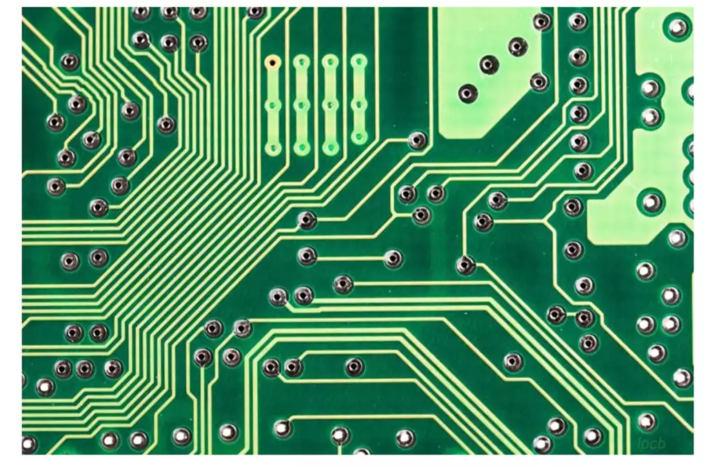
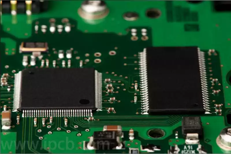
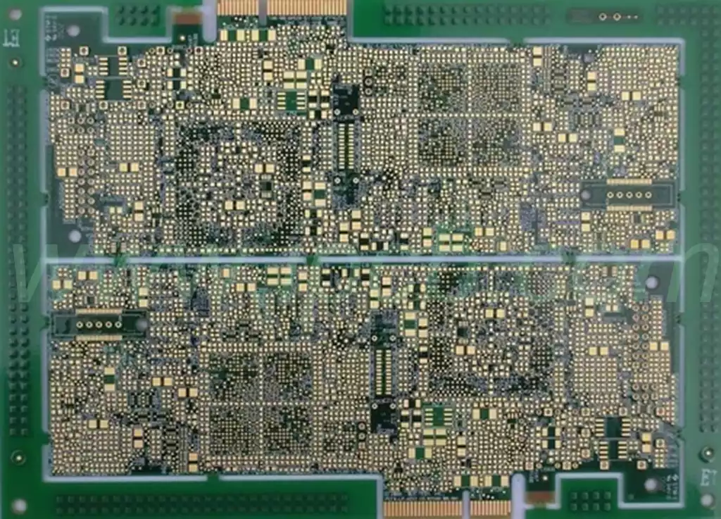
A copper substrate PCB is used when an electronic assembly must transfer concentrated heat away from power components more effectively than a conventional FR4 board can. The solid copper base spreads heat across the board and provides a short thermal path toward the enclosure, cold plate or external heat sink. However, replacing FR4 or aluminum with copper does not automatically solve a thermal problem. The dielectric layer between the circuit and the metal base can still become the dominant thermal barrier. The real engineering question is therefore not whether copper conducts heat well. It is whether the complete board structure can move heat from the component junction through the solder joint, copper circuit, insulating dielectric, copper base and mechanical interface without creating excessive temperature rise or compromising electrical isolation.
The term copper substrate PCB usually describes a type of insulated metal substrate rather than an ordinary FR4 board covered with copper foil. A typical construction contains a patterned copper circuit layer, a thin electrically insulating but thermally conductive dielectric and a thick copper base. These layers perform different functions. The upper circuit layer carries current and provides component pads. The dielectric electrically separates the circuit from the metal base. The copper base spreads heat, increases mechanical rigidity and transfers thermal energy toward the final cooling structure. This construction should not be confused with a copper-clad FR4 PCB. Nearly every conventional PCB uses copper foil to form its traces, but that does not make it a copper base PCB. It is also different from direct bonded copper ceramic substrates, in which copper is bonded to materials such as alumina, aluminum nitride or silicon nitride. DBC and AMB substrates are generally selected for more demanding power-module conditions involving high voltage, high temperature and thermal cycling. Rogers describes these structures as pure copper bonded or brazed to ceramic rather than as a polymer-dielectric metal-core board. Rogers curamik substrate information.
The copper base is highly conductive, but heat cannot reach it without crossing the dielectric. This makes dielectric performance the central design issue in a copper substrate PCB. A thick copper base can distribute heat once it reaches the metal, but it cannot compensate for a poorly selected insulating layer. If the dielectric is too thick, has insufficient thermal conductivity or contains voids, heat remains concentrated near the component. The external surface of the copper base may appear relatively cool while the semiconductor junction is already operating at an unsafe temperature. The dielectric must satisfy two opposing requirements. It should be thin enough to reduce thermal resistance, yet strong enough to maintain electrical isolation under the operating voltage, manufacturing tolerances and long-term environmental stress. Selecting only the material with the highest published thermal conductivity can be misleading because actual performance also depends on dielectric thickness, interface quality and the area through which heat enters the layer. For this reason, the dielectric should be selected according to the complete application rather than a single data-sheet value. The review needs to consider operating voltage, transient voltage, required isolation, component heat density, board area, expected temperature range and the consequences of local dielectric defects. Henkel’s thermal-insulator information similarly treats thermal conductivity and dielectric strength as simultaneous material requirements rather than interchangeable specifications. Henkel thermal insulation materials.
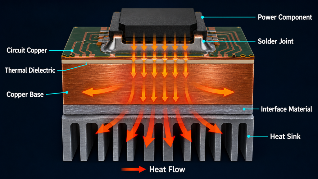
Copper thickness above the dielectric also matters. A wider copper area around a power device spreads heat before it crosses the insulating layer. This reduces the concentration of heat entering the dielectric directly beneath a small package. The copper base then continues spreading that energy laterally after it passes through the insulation. The most effective thermal path is therefore not created by the base metal alone. A reliable copper substrate PCB combines suitable component-pad geometry, adequate circuit copper, a controlled dielectric and close mechanical contact between the base and the final cooling surface.
Copper becomes useful when heat is highly concentrated, operating current is high or the board has limited area for spreading thermal energy. Common examples include high-power LED assemblies, motor drives, solid-state relays, power converters, charging systems and industrial control modules. In these products, a copper substrate PCB can provide better lateral heat spreading than an aluminum-base structure of similar geometry. It can also support high-current conductors and reduce local temperature differences across the board. Copper is particularly valuable when several power devices share the same cooling surface but do not dissipate equal amounts of heat. The advantage becomes less important when the main thermal bottleneck exists somewhere else. Poor contact between the board and enclosure, an uneven mounting surface, insufficient airflow or a badly selected thermal interface material can prevent the copper base from transferring heat into the surrounding structure. In that situation, changing only the substrate material may increase cost and weight without producing a meaningful reduction in component temperature. A copper base is also not automatically necessary for every warm circuit. If power is distributed across a large board and component temperatures remain within their limits, an aluminum metal core PCB or a carefully designed FR4 board with thermal vias may be sufficient. Copper should be selected when thermal simulation, prototype measurement or previous field data shows that the additional spreading performance is required.
After the material system has been selected, layout determines how effectively the board uses it. Heat-generating devices should have sufficient copper area around their thermal pads. Narrow conductor necks can restrict both current and heat flow, while solder-mask-defined regions may reduce the effective area available for heat transfer. Power devices placed very close together can create overlapping thermal zones. Even if each component appears acceptable when evaluated individually, their combined heat can raise the temperature of the shared substrate. Moving devices apart may improve heat distribution, but excessive separation can increase switching-loop area and electrical noise. The final placement must balance thermal spreading with electrical performance. A copper substrate PCB used in a switching power circuit still requires compact current loops, appropriate gate-drive routing and controlled separation between noisy switching nodes and sensitive control signals. Thermal performance cannot compensate for poor electrical layout. Mounting holes also affect the heat path. Fastener location determines how evenly the board presses against the enclosure or heat sink. Too few mounting points can allow the substrate to lift locally, creating an air gap beneath a power device. Excessive or uneven clamping can bend the assembly and stress solder joints. The interface beneath the board should be treated as part of the design. Surface flatness, insulation requirements, thermal-interface thickness and assembly pressure all affect the connection between the copper base and the cooling structure. The contact area should be verified on the real mechanical assembly rather than assumed from the PCB outline.
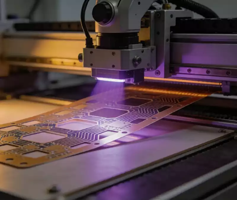
Copper is heavier and more difficult to machine than aluminum or FR4. Its thermal mass also changes how the board responds during soldering. These characteristics affect routing, drilling, panel handling and reflow profiling. Tool wear and edge quality require attention during fabrication. Burrs around routed edges or mounting holes can interfere with mechanical contact and may create electrical-clearance risks. Because the metal base is conductive, the required separation between circuit features, holes and exposed substrate must be defined clearly in the manufacturing data. A copper substrate PCB may also heat more slowly during assembly because the base draws energy away from the component side. A generic reflow profile can leave large thermal pads incompletely soldered even when smaller components appear normal. Increasing oven temperature without measurement is not a safe solution because small components may then experience excessive thermal exposure. The reflow profile should be verified at representative locations. Temperature measurements are particularly important near large power packages, dense copper areas and components with limited thermal tolerance. Solder-paste aperture design must also account for the thermal pad geometry and the possibility of component float or excessive voiding. Panelization deserves separate review. The weight and rigidity of a copper base can affect conveyor support and depanelization. Breakaway structures suitable for FR4 may not produce a clean or economical result with thick copper. The manufacturer should determine the panel method according to substrate thickness, board outline and available machining equipment.
The copper base is conductive, even when the product treats it as a mechanical heat spreader. Any failure in the insulating dielectric can connect the circuit to the enclosure or heat sink. This makes isolation testing essential in high-voltage applications. Electrical verification should match the product’s working voltage and safety requirements. Testing only continuity on the circuit layer does not confirm the integrity of the insulation between the circuit and the base. The manufacturing plan may need dielectric-withstand testing, insulation-resistance testing or both. Clearance around mounting holes requires particular attention. Metal fasteners, washers and enclosure features can approach the circuit layer more closely than expected. If mounting hardware connects the copper base to protective earth or the chassis, the relationship must be defined in the schematic and mechanical drawings. A damaged edge can also expose a conductive path. The final inspection should therefore include routed edges, holes and any region where machining approaches the dielectric boundary.
Prototype evaluation should measure component temperature under realistic electrical and mechanical conditions. Testing the bare assembly on an open bench may produce a different result from testing it inside the final enclosure. Power level, airflow, mounting pressure and ambient temperature should represent actual use. Temperature measurement should include the power component, the surrounding circuit area and the copper base near the cooling interface. A thermal image can identify spreading patterns, but component case temperature alone does not directly reveal semiconductor junction temperature. The component manufacturer’s thermal data and operating limits still need to be considered. The prototype should also experience repeated heating and cooling. Copper, polymer dielectric, solder and component packaging expand at different rates. Thermal cycling can expose problems that do not appear during a short functional test, including solder fatigue, dielectric separation and changes in mechanical contact. Before production, iPCB can review the copper base material, dielectric specification, board geometry, fabrication limits, assembly profile and inspection requirements as one manufacturing system. This prevents the selected material from being separated from the processes needed to manufacture it reliably.
A copper substrate PCB is justified when concentrated heat, high current or limited board area requires more heat spreading than FR4 or an aluminum base can provide. Its performance, however, depends on much more than the conductivity of copper. The dielectric controls how heat reaches the base, layout controls where heat enters the structure, and the mechanical interface controls whether that heat can leave the board. Fabrication, soldering and isolation testing must then preserve those design intentions during production. Choosing a copper substrate PCB should therefore follow thermal analysis and prototype measurement, not the assumption that copper is always the best PCB material. When the complete heat path is designed and verified together, a copper substrate PCB can reduce component temperature and support reliable high-power operation without adding unnecessary material cost.