A PCB panel allows multiple circuit boards to move through solder-paste printing, component placement, reflow, inspection and testing as one mechanically stable unit. Good panelization improves manufacturing efficiency, but fitting as many boards as possible into one rectangle is not enough. A panel can achieve high material utilization and still create placement errors, board vibration, solder-joint damage or difficult depaneling. The main design problem is maintaining sufficient rigidity throughout assembly without applying excessive stress when the individual boards are separated. Every PCB panel must therefore be designed around the complete production flow rather than the bare-board outline alone.
A panel is a manufacturing array containing several copies of the same PCB or a controlled mixture of different designs. Individual boards are held together by panel rails, routed tabs, V-score lines or a combination of these features. The outer rails provide space for conveyor handling, tooling holes, fiducials, identification marks and process coupons. Internal support structures keep the boards from moving or bending while the assembly passes through production equipment. Panelization may be completed by the PCB designer, fabricator or assembly manufacturer. The correct owner depends on the project. A simple rectangular design may only require the fabricator’s standard array, while a densely assembled board with edge connectors, overhanging components or strict depaneling limits requires coordination between PCB fabrication, assembly and mechanical engineering.
Material utilization affects PCB cost because unused laminate inside the manufacturing panel becomes scrap. Increasing the number of boards per array can reduce the fabrication cost per unit, but maximum nesting density is not always the lowest-cost solution after assembly is considered. A narrow or poorly supported PCB panel may flex during solder-paste printing. Stencil pressure can push the center of the array downward, changing the contact between the stencil and component pads. The resulting paste deposits may be acceptable near the rails but inconsistent near the unsupported center. The same panel can vibrate during high-speed component placement. Small passive components are placed rapidly, and any movement between the machine support table and the PCB surface reduces positional consistency. The problem becomes more serious when the panel combines large cutouts, thin boards or uneven board orientations. Thermal behavior also changes across the array. Large copper areas and densely populated circuits absorb more heat than empty regions. When different board designs are mixed without considering copper distribution and component mass, the reflow process may produce uneven soldering results. A production-ready PCB panel balances material utilization against three process requirements: sufficient rigidity during printing and placement, predictable heating during reflow, and controlled separation after assembly. The best array is not necessarily the one containing the largest number of circuits. It is the one that achieves acceptable material cost without introducing avoidable assembly defects or difficult handling.
Panel rails create a consistent surface for conveyors, clamps and handling equipment. They also keep components away from machine contact areas. Without suitable rails, a small or irregularly shaped board may not travel reliably through an automated SMT line. Rail width is not universal. It depends on the assembler’s conveyor, stencil printer, support tooling and component overhang. The rail must be wide enough to remain rigid after routing while providing sufficient room for fiducials and tooling holes. A PCB panel may require rails on two sides when the assembly line only needs conveyor support along the travel direction. Four-sided rails provide greater rigidity and more tooling space but consume additional material. Thin boards, small circuits and arrays with large routed openings often benefit from a complete frame. Copper features should not unintentionally enter the rail unless they serve a defined purpose. Exposed copper near tooling locations can interfere with electrical isolation or become damaged during handling. The fabrication data should clearly distinguish permanent circuit features from disposable panel structures. Reference text, order numbers and barcodes can be placed on the rails, but they should remain outside machine contact areas. Any marking needed for traceability must remain readable through assembly and test.
Fiducials provide optical reference points for the solder-paste printer and pick-and-place equipment. They allow the machines to identify panel position, rotation and dimensional variation before processing begins. At least three appropriately distributed global fiducials are commonly used to establish the coordinate system of the complete PCB panel. Local fiducials may also be required near fine-pitch BGAs, QFNs or connectors when component-placement accuracy cannot rely only on the outer references. Eurocircuits recommends at least three fiducials on the panel frame and notes that individual boards in a multi-board panel can use local fiducials to improve registration accuracy. A fiducial is not merely a circular copper pad. Its surrounding area must remain clear of copper, solder mask, silkscreen and components so that the vision system can identify a clean contrast boundary. Placing a reference mark close to a similar circular pad or reflective metal feature can reduce recognition reliability. The references should not be positioned in a perfectly symmetrical arrangement. An asymmetric pattern helps equipment detect incorrect panel orientation. This is particularly useful when the board design itself appears symmetrical but contains polarity-sensitive components. Tooling holes serve a different purpose. They provide mechanical location or fixture alignment and should not be treated as optical fiducials. Their diameter, position and tolerance must correspond to the equipment or fixture that will use them.
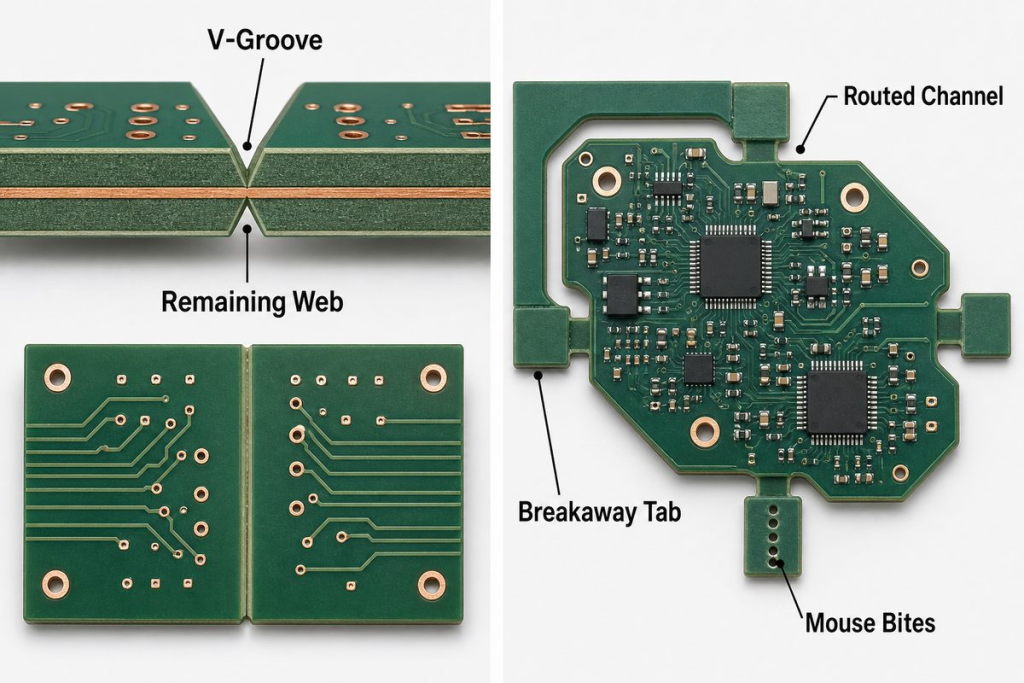
The separation method has the greatest direct effect on the final mechanical risk. V-scoring and tab routing are not interchangeable solutions. V-scoring works best with straight board edges. A V-score cuts matching grooves into the top and bottom surfaces, leaving a controlled section of material between adjacent boards. After assembly, the boards are separated along the weakened line. This method is efficient for rectangular boards arranged in continuous rows. It uses little space between circuits and makes panelization economical. However, a score line normally travels across the complete panel, so it is not suitable for every irregular outline or interrupted separation path. The remaining material must keep the array rigid during assembly while still allowing controlled separation. If the residual thickness is too large, depaneling requires excessive force. If it is too small, the panel may bend or break during handling. Components, vias and copper features must remain far enough from the score line to avoid mechanical damage. The exact clearance should follow the fabricator’s scoring capability, board thickness, component type and depaneling equipment. IPC-2222 includes design considerations for scoring clearance and breakaway structures, while actual production values still need confirmation with the selected manufacturer. Manual bending creates strain that travels beyond the visible separation line. Ceramic capacitors are particularly vulnerable because their rigid bodies can crack when the PCB bends. A power inductor, connector or BGA located near the edge may also experience solder-joint stress even when no immediate damage is visible. For assemblies with sensitive components close to the board edge, a controlled V-score cutting machine is safer than breaking the array by hand.
Tab routing uses a milling tool to cut most of the individual board outline while leaving narrow bridges that hold the circuits in the PCB panel. Small drilled perforations, often called mouse bites, may be added to control where each tab breaks. This method supports curved outlines, internal cutouts and boards that cannot share continuous straight edges. It also provides more freedom when the boards require different orientations. The disadvantage is reduced panel stiffness. Routing removes material, and a large number of open channels can allow individual boards to move during printing or placement. Tab number and location must therefore be selected according to board size, weight and component distribution. A heavy connector should not be supported by one distant tab while the surrounding outline is completely routed. The board may rotate or vibrate during placement. Tabs should stabilize the circuit without being positioned where removal will damage edge components or leave an unacceptable protrusion. Mouse-bite holes should break toward the disposable material rather than extending unnecessarily into the finished outline. If the final enclosure requires a smooth board edge, secondary trimming or routing may be needed after separation. Eurocircuits describes break routing as milling around the PCB profile while leaving deliberately positioned tabs to maintain panel stability. Its guidance also distinguishes this method from V-scoring, which is primarily suited to continuous straight separations.
Component-to-edge clearance cannot be determined only by whether the package fits inside the board outline. The component also needs protection from cutting tools, board bending and operator handling. Large ceramic capacitors, BGAs, QFNs and fragile connectors require particular attention. Their distance from the separation line should reflect the expected strain and the selected depaneling method. Component orientation can also matter. A long ceramic capacitor positioned parallel to a bending line may respond differently from one rotated relative to that line. Overhanging connectors create another constraint. A connector extending beyond the finished PCB outline may collide with an adjacent board or panel rail. The panel may require an empty region, locally removed rail or altered board orientation to create assembly clearance. Tall components can interfere with depaneling equipment after reflow. A separation path that appears accessible in the bare-board drawing may become blocked after transformers, heat sinks or terminal blocks are installed. The PCB panel should therefore be reviewed using the complete 3D assembly, not only the Gerber outline. This review should include the depaneling blade, router bit or support fixture that will approach the finished assembly.
Placing several different designs in one panel can reduce material cost for prototypes or product families, but it introduces production complications. Different boards may use different stencil requirements, component densities or test procedures. If one design requires a process change, the complete array may be affected. A failed circuit can also complicate traceability when test data is recorded at panel level rather than by individual board position. Mixed boards should share compatible laminate, thickness, copper weight, surface finish and assembly conditions. Their orientation should support the same soldering process, and each circuit must have a stable position identifier. A mixed PCB panel is most practical when the boards belong to one product and are assembled together in predictable quantities. Combining unrelated boards only to fill empty laminate may reduce bare-board cost while increasing assembly setup, sorting and inventory complexity.
Panel drawings should identify the overall dimensions, rail width, board orientation, separation method, tooling-hole positions, fiducials and individual board references. Routed regions and V-score lines must be represented unambiguously. The data package should also state whether the customer or manufacturer controls the panelization. Sending both an individual-board outline and an unexplained pre-panelized Gerber can create duplicate routing or conflicting dimensions. Centroid data must use the same origin and orientation as the assembly panel. Each reference designator should remain unique or be connected to a defined circuit position. Test records should identify both the panel and the individual board location so that repeated defects can be associated with a specific region of the array. Fabricators also use their larger production panels for tooling holes, process coupons, identification and manufacturing control. This fabrication panel is not always identical to the customer’s assembly array. Eurocircuits explains that production-panel borders support manufacturing equipment and may contain tooling holes, fiducials, test coupons and barcodes. Before releasing a PCB panel, the assembly manufacturer should confirm permitted panel dimensions and thickness, required conveyor-edge clearance, rail and tooling-hole requirements, fiducial size and clearance, stencil and support-fixture compatibility, depaneling method, and component clearance from separation lines. These are machine- and process-dependent values. Copying dimensions from a previous project is unsafe unless the board construction and assembly conditions are genuinely equivalent.
Panel problems become expensive after the stencil, SMT program and test fixture have been created. A DFM review should therefore evaluate the array before tooling is released. The review should simulate how the PCB panel will be supported during printing, placement, reflow, inspection, testing and separation. Weak regions, blocked cutting paths and components exposed to bending should be corrected in the panel design rather than managed through operator skill. For projects moving from prototype to repeat production, iPCB can coordinate bare-board fabrication, panel design, SMT requirements and depaneling within the same manufacturing review. This helps prevent a panel optimized by the fabricator from creating difficulties later on the assembly line.
An effective PCB panel does more than increase the number of circuits processed at one time. It creates a mechanically stable platform for accurate printing and placement, provides reliable machine references and allows individual boards to be separated without damaging components or solder joints. Material utilization remains important, but it should not override rigidity, tooling access or depaneling safety. The best PCB panel is the one designed around the real production equipment and the mechanical behavior of the assembled boards. When rails, fiducials, separation features and component clearances are reviewed as one system, a PCB panel reduces handling time and manufacturing cost without transferring hidden mechanical risk into the finished product.