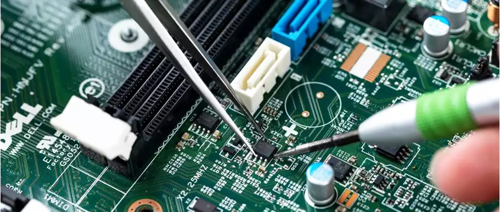
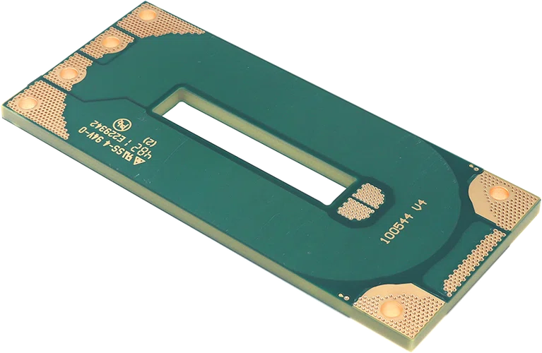
A solar panel PCB board is a printed circuit board used in photovoltaic systems to control, monitor, protect, or convert the electrical energy generated by solar panels. Depending on the system architecture, the PCB may be used in a microinverter, solar inverter, MPPT controller, combiner box, monitoring unit, or other power electronics connected to the photovoltaic system.
Unlike a general-purpose PCB, a solar panel PCB board may need to operate continuously under high electrical loads, temperature variations, humidity, electrical noise, and outdoor environmental conditions. Its design therefore depends heavily on voltage, current, thermal conditions, isolation requirements, switching frequency, and the specific function of the photovoltaic equipment.
Where Solar Panel PCB Boards Are Used
Solar panel PCB boards appear throughout the photovoltaic power conversion and monitoring chain. The most important applications include microinverters, string inverters, central inverters, MPPT controllers, combiner boxes, monitoring equipment, rapid-shutdown equipment, and power optimizers.
Microinverter PCBs are installed in systems where power conversion is performed close to individual PV modules. The board must combine switching power electronics with sensing, control, protection, and communication functions within a relatively compact assembly.
String and central inverter PCBs operate at higher system levels. They may contain MPPT circuits, DC-link circuits, inverter bridges, gate drivers, voltage and current sensing, protection circuits, communication interfaces, and grid-interconnection control. Larger inverter architectures may distribute these functions among separate power and control boards rather than placing everything on one PCB.
Combiner box and monitoring PCBs serve a different purpose. They can monitor PV strings, measure voltage or current, provide communication with the inverter, and support protection and fault-detection functions. In industrial and utility-scale photovoltaic systems, PCB-based electronics may also be found in tracker controllers, monitoring nodes, and other control equipment.
How a Solar Panel PCB Board Works
The operation of a solar panel PCB board depends on its position within the photovoltaic system.
A PV module generates DC electricity. When the system uses an inverter, the electronic circuitry receives the variable DC input and processes it through power conversion stages. An MPPT control system determines an appropriate operating point for the PV source, while switching devices regulate energy transfer through the converter. The inverter stage can then convert DC into controlled AC for the grid or connected loads.
The PCB provides the physical electrical paths between these circuits. Copper traces and planes carry current, while control traces transmit sensing and switching signals. Power semiconductors, capacitors, inductors, transformers, sensors, controllers, and protection components are positioned according to the electrical topology and thermal requirements.
In a high-power inverter, the PCB may therefore perform several functions simultaneously: power distribution, gate-drive control, voltage and current measurement, fault protection, communication, and thermal management.
Key Design Requirements for Solar Panel PCB Boards
High Current Carrying Capacity
Power conversion circuits can carry substantially more current than typical digital control electronics. PCB designers must therefore select copper thickness, trace width, copper planes, vias, terminals, and other conductive structures according to the actual current and allowable temperature rise.
Heavy copper can reduce conductor resistance and help distribute heat, but simply increasing copper thickness is not a substitute for proper thermal and electrical design. Current density, copper geometry, component losses, connector ratings, and heat dissipation must be considered together.
High Voltage Insulation
Photovoltaic power electronics can operate at high DC voltages. Depending on the system architecture, PV equipment can involve hundreds or more than 1,000 VDC. This makes creepage, clearance, insulation, slots, component spacing, and contamination conditions important parts of PCB design.
High voltage PCB layout cannot be treated simply as a matter of increasing trace spacing. The required distances depend on the working voltage, overvoltage environment, insulation system, pollution conditions, materials, and applicable safety requirements.
Thermal Management
Solar equipment may operate for long periods while exposed to elevated ambient temperatures. Power semiconductors, inductors, capacitors, resistive elements, and other components generate heat during operation.
The PCB must therefore provide a practical thermal path from heat-generating components to the heatsink, enclosure, or surrounding structure. Copper planes, thermal vias, component placement, board thickness, heat spreaders, and mechanical interfaces can all influence thermal performance.
For high-power designs, thermal analysis should begin during PCB layout rather than after the prototype has already been assembled.
Electromagnetic Compatibility
Solar inverters use switching power electronics that generate high dv/dt and di/dt transients. Poor PCB layout can create excessive electromagnetic interference, ringing, ground bounce, and measurement errors.
High-current switching loops should be kept compact, sensitive analog measurement circuits should be separated from noisy power paths, and gate-drive circuits should be positioned with the switching devices they control. Grounding and return-current paths must also be considered rather than focusing only on the forward signal trace.
Environmental Reliability
Solar equipment may operate in environments with large temperature changes, humidity, dust, condensation, and other environmental stresses. The PCB assembly must therefore be designed according to the actual enclosure and operating environment.
Depending on the application, conformal coating, sealing, appropriate component selection, corrosion protection, and contamination control may be required. These measures should be selected according to the actual environmental conditions rather than applied universally to every solar panel PCB board.
Materials Used for Solar Panel PCB Boards
Standard FR-4 can be suitable for many solar control and monitoring boards, but higher-performance materials may be required for power conversion applications.
Material selection depends on operating temperature, voltage, thermal requirements, mechanical construction, frequency, and reliability targets. High-Tg laminates can be useful where the board experiences significant thermal cycling, while metal-core or other thermal-management structures may be considered when heat removal is a dominant design constraint.
The material should also be evaluated together with the complete stackup. Dielectric thickness influences insulation, capacitance, impedance, and mechanical construction, so selecting a laminate only by its nominal Tg or cost does not provide a complete PCB design solution.
Solar Panel PCB Board Manufacturing Process
Manufacturing begins with the PCB design data and material selection. The manufacturer then produces the required copper layers, drills the board, forms plated interconnections, applies solder mask and surface finish, and performs electrical inspection and testing.
For multilayer solar power boards, inner-layer fabrication and lamination require accurate registration and controlled copper distribution. Drilling and plating must provide reliable interconnections between conductive layers, while the outer-layer pattern must support the required current and component connections.
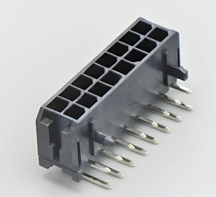
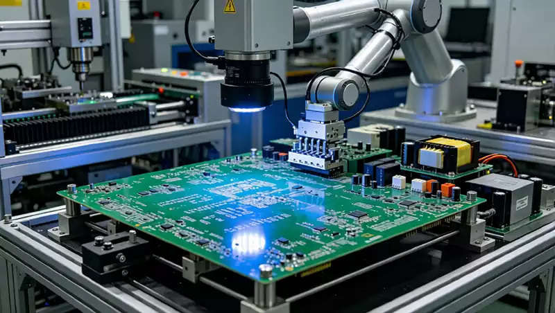
PCB assembly introduces another set of requirements. Power semiconductors, capacitors, connectors, transformers, and other components may require a combination of SMT and through-hole assembly. The assembly process must account for component size, thermal mass, solder-joint reliability, and mechanical stress.
The U.S. Department of Energy describes PV power electronics manufacturing as including PCB assembly, component placement, soldering, coating, and enclosure integration, illustrating that the PCB is one part of the broader photovoltaic electronics system.
Testing Solar Panel PCB Boards
Testing requirements depend on the function and voltage level of the board. Typical production and validation activities may include automated optical inspection, electrical testing, component verification, functional testing, insulation testing, and power-up testing.
High-voltage boards require particular attention to isolation and safety testing. Functional testing may also verify MPPT operation, voltage and current measurement, gate-drive signals, communication interfaces, protection responses, and inverter control behavior.
For production, test points and accessible measurement nodes should be considered during PCB design. Design for Test can reduce the difficulty of diagnosing failures and improve production consistency.
Solar Panel PCB Board Reliability Considerations
Reliability is strongly influenced by the interaction between electrical, thermal, mechanical, and environmental stresses.
A solar panel pcb board may operate correctly during a short laboratory test but experience failures after repeated thermal cycling or long periods of high electrical load. Solder joints, vias, connectors, capacitors, semiconductor junction temperatures, and PCB materials can all contribute to long-term reliability.
For this reason, reliability evaluation should consider the actual operating profile rather than relying only on nominal component ratings. Continuous power operation, overload conditions, switching transients, temperature cycling, humidity, vibration, and surge exposure may all be relevant depending on the application.
How to Choose a Solar Panel PCB Design
The PCB should be specified from the electrical architecture rather than from the keyword “solar PCB” alone.
Start with the maximum and nominal input voltage, continuous and peak current, power level, switching frequency, operating temperature, expected service environment, and required isolation. Then determine the PCB layer count, copper thickness, material system, thermal structure, connector technology, component package strategy, and manufacturing process.
The design should also define inspection and testing requirements before production. For a power board, electrical safety and functional testing can be as important as dimensional tolerances and cosmetic quality.
A manufacturability review should be performed before releasing the design. Trace geometry, copper distribution, hole structures, component clearances, thermal interfaces, assembly access, and test points can all affect production yield and long-term reliability.
A solar panel PCB board is not simply a standard PCB placed inside a solar product. Its construction must be matched to the electrical and environmental demands of photovoltaic equipment.