A pcb doppler radar combines RF circuitry, signal processing, antenna structures, and power management on a printed circuit board. In this type of system, the PCB is more than a platform for mounting components. Trace geometry, dielectric thickness, grounding, component placement, antenna structure, and manufacturing tolerances can all influence how RF energy moves through the board. A radar circuit that performs well in simulation can therefore behave differently after it is transferred to a physical PCB.
This becomes particularly important in Doppler radar because the receiver may need to detect a relatively small frequency shift from a reflected signal while the transmitter is operating nearby. Unwanted coupling, power-supply noise, transmission-line loss, or antenna mismatch can make the received signal harder to process. The PCB has to preserve the intended RF paths while keeping interference under control.
When PCB Layout Becomes Part of the Radar Circuit
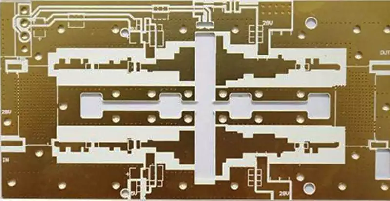
In a conventional low-frequency circuit, a PCB trace can often be treated simply as a connection between two components. At RF frequencies, that assumption becomes unreliable. The physical dimensions of a transmission line and its relationship to the reference plane determine its electrical characteristics. Factors such as trace width, conductor thickness, distance to the ground plane, and dielectric properties all affect transmission-line impedance.
This means the RF section of a pcb doppler radar needs to be designed around controlled transmission lines rather than ordinary point-to-point routing. The connection between an RF source, amplifier, filter, mixer, and antenna can introduce loss or impedance discontinuities if its geometry changes unexpectedly. Bends, layer transitions, connectors, vias, and component footprints can all become part of the RF path.
The reference plane matters just as much. A stable ground structure provides a predictable return path and helps maintain the intended transmission-line environment. If the return path is interrupted by unnecessary gaps or poorly planned transitions, the actual electromagnetic behavior can differ from what was assumed during the design process.
This is also why reproducing an RF reference design involves more than copying the schematic. When an RF device manufacturer provides a recommended layout, the trace geometry, stackup relationship, component placement, and surrounding ground structure may all contribute to the expected performance.
Why the Receiver Is Sensitive to Board-Level Interference
The receiver is where PCB-related problems can become particularly noticeable. A Doppler radar has to distinguish the desired reflected signal from signals that already exist inside the hardware. The transmitter, receiver, local oscillator, mixer, power supply, and digital circuitry can all become sources of unwanted energy.
Tx and Rx routing therefore deserves deliberate physical planning. RF lines that run close together can couple energy from one path into another, while digital clocks and other fast-changing signals can introduce interference into sensitive RF circuitry. The objective is to reduce unwanted coupling while maintaining controlled signal and return-current paths.
The problem is not limited to traces. Components themselves can create coupling paths. A transmitter placed immediately beside a sensitive receiver may leak energy through the air, package structures, power network, or PCB copper even when there is no direct schematic connection between the two sections.
A practical pcb doppler radar can therefore benefit from treating the board as several electrically different regions. The RF transmit path, receive path, signal-processing section, and power circuitry should have a deliberate physical relationship. This does not necessarily mean dividing the ground plane into isolated sections. In many RF designs, maintaining a continuous reference plane and controlling current paths can be more effective than creating arbitrary ground islands.
The placement sequence should also follow the actual signal flow. RF components should be positioned so that critical connections remain short and predictable, while sensitive receiver circuitry is kept away from obvious noise sources. This reduces the number of opportunities for unwanted coupling before the signal even reaches the processing stage.
The Antenna Depends on the PCB Around It
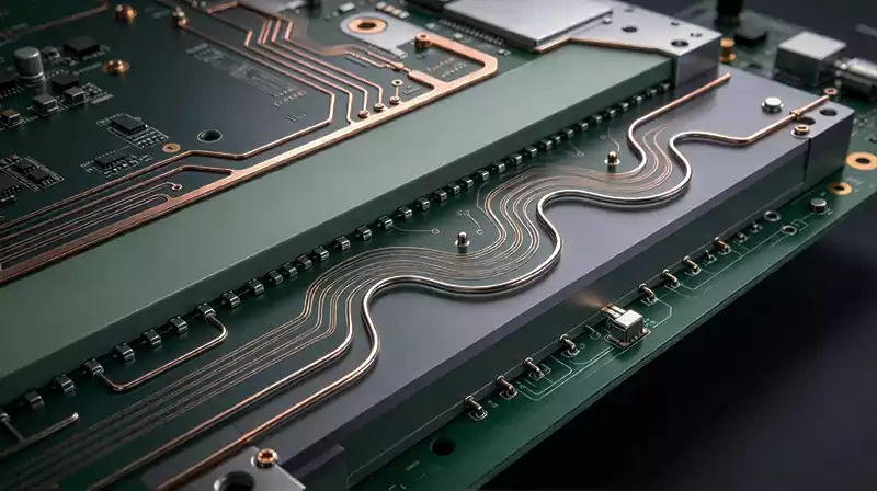
When the antenna is integrated directly into the circuit board, the relationship between the antenna and PCB becomes even more important. The antenna does not operate independently from the substrate, copper layers, ground structure, and surrounding objects. Changing the dielectric thickness or nearby copper can change the electromagnetic environment seen by the antenna.
The feed line between the RF circuit and antenna must therefore be treated as part of the antenna system. An impedance mismatch can reduce the amount of RF power reaching the antenna during transmission and can also affect the signal received by the receiver.
The antenna location matters as well. Nearby copper, connectors, shielding structures, mechanical parts, and other RF circuits can affect radiation characteristics or create additional coupling paths. Systems with multiple transmit and receive antennas face another challenge because compact placement can increase mutual coupling.
For this reason, antenna keepout areas should be established before the rest of the board is routed. The mechanical enclosure should also be considered early if the antenna is integrated into the PCB. A board that works correctly on a laboratory bench may behave differently after being installed next to a housing, bracket, battery, shield, or other conductive structure.
In a pcb doppler radar, the antenna and its surrounding PCB geometry should therefore be considered as one RF structure. Treating the antenna as an isolated component can lead to unexpected changes once the complete board is manufactured and assembled.
Stackup and Materials Can Change RF Behavior
The PCB stackup determines the physical relationship between RF traces and their reference planes. That relationship directly affects controlled impedance, while the dielectric material contributes to signal loss and propagation characteristics.
For a pcb doppler radar, the stackup should be established before detailed RF routing begins. A designer cannot reliably define a transmission line simply by specifying a target trace width without knowing the dielectric thickness and material characteristics around it.
This becomes increasingly important as operating frequency rises. A stackup that is adequate for a low-frequency control section may not provide the same RF performance when used for microwave circuitry. Some radar designs therefore use materials and layer structures selected specifically for the critical RF paths, while other sections of the board are designed around their own electrical and manufacturing requirements.
Copper geometry matters as well. A change in conductor width or dielectric thickness changes the electrical characteristics of the transmission line. Manufacturing variation can therefore become an RF issue rather than merely a dimensional issue.
Thermal behavior should also be considered. RF power amplifiers and other active components can generate significant heat, while temperature changes can affect electrical characteristics. Copper areas, thermal vias, component placement, and the surrounding mechanical structure can all influence temperature distribution across the board.
Designing the PCB Around the Signal You Need to Detect
The most useful way to approach a pcb doppler radar is to start with the signal that the receiver needs to detect and work backward through the system. The question is not simply whether each component is connected correctly. It is whether the PCB preserves the relationship between the transmitted signal, reflected signal, RF conversion stages, and final Doppler output.
That changes how the layout should be evaluated. RF paths need controlled impedance. Tx and Rx sections need appropriate isolation. The receiver needs a clean electrical environment. Antenna structures require suitable surrounding geometry. Power circuits must be prevented from introducing unnecessary noise. The stackup needs to match the assumptions used during RF design and simulation.
Prototype testing can then be used to compare the manufactured board with the expected behavior. Measurements of RF paths, antenna performance, receiver output, noise, and Doppler response can reveal problems that are difficult to identify from the schematic alone.
The key point is that the PCB is part of the radar system. Once the operating frequency is high enough for board geometry to affect RF behavior, layout decisions become electrical decisions. For a pcb doppler radar, controlling these physical details is essential for achieving predictable sensitivity, isolation, signal quality, and repeatable performance.