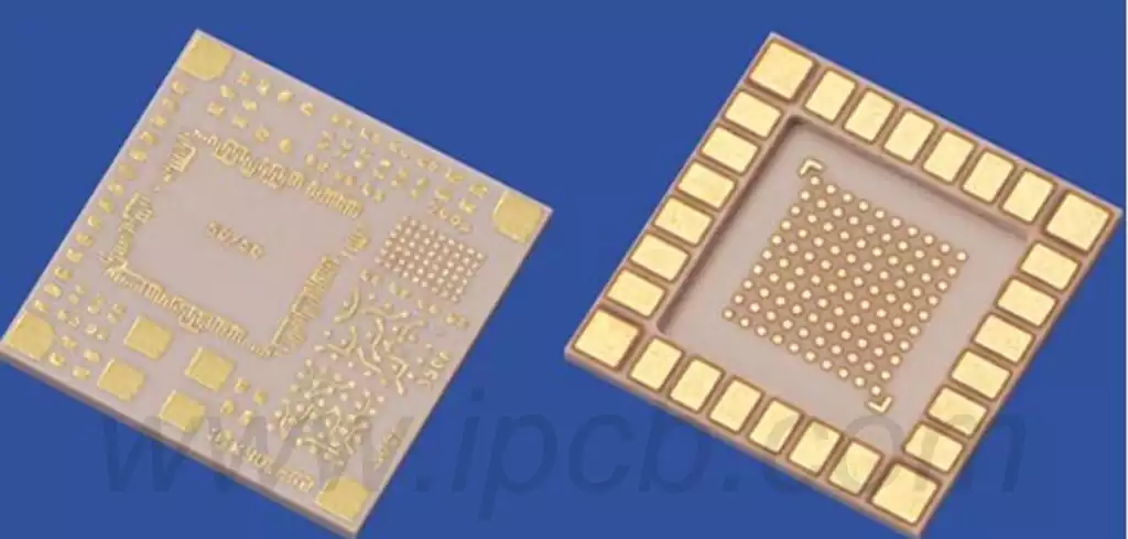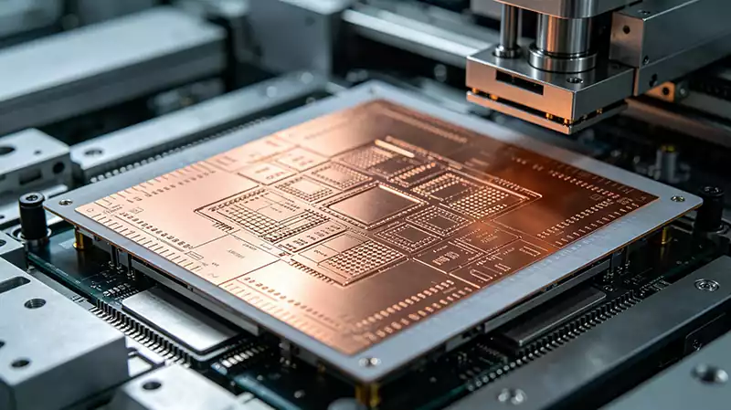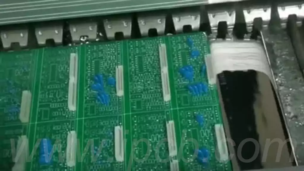
A pcb clone is a reproduction of an existing printed circuit board intended to preserve its physical fit, electrical connections, and functional behavior. It is useful when original design files are unavailable, a circuit board has been discontinued, or replacement hardware is needed for equipment that must remain in service. Rather than designing a completely new circuit from scratch, engineers use an existing board as the reference for recovering its construction and manufacturing requirements.
Creating a reliable pcb clone involves more than matching the board’s outline or copying visible copper traces. Component specifications, internal layers, via structures, material properties, and firmware-dependent functions may all affect whether the replacement operates correctly. The objective is to produce a board that meets defined requirements and can be verified against the original, not merely one that looks similar.
When Is a PCB Clone Needed?
One common application is replacing obsolete circuit boards. Industrial control equipment, communication systems, testing instruments, and specialized electronic products may remain operational long after their original boards become difficult to source. A properly verified replacement can help extend equipment service life without requiring an immediate redesign of the entire system.
A pcb clone may also be useful when the physical board is available but its original Gerber files, schematic, bill of materials (BOM), or assembly documentation have been lost. Recovering these details can make it possible to manufacture replacement boards and maintain a documented production process.
In some projects, engineers need a replacement that fits the existing enclosure and connects to the same cables, connectors, and mounting points. This requires accurate mechanical measurements as well as electrical reconstruction. Even a small change in connector location, board thickness, or mounting-hole position may prevent the replacement from fitting correctly.
The required outcome should be defined before work begins. A bare-board replacement requires fabrication data and verification of the PCB itself. A fully assembled replacement may also require component identification, sourcing, soldering, programming, and functional testing. If the intention is to modify or improve the original design, a broader reverse-engineering and redesign project may be more appropriate than a direct clone.
How a PCB Clone Is Developed
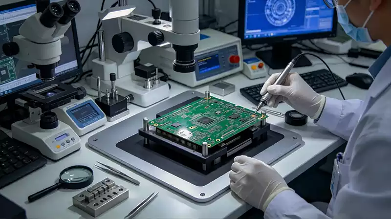
The process begins with a detailed inspection of the reference board. Engineers document its dimensions, layer count where known, component markings, connector positions, mounting features, visible copper patterns, and overall construction. Existing schematics, product documentation, and component datasheets can help resolve missing information and reduce unnecessary investigation.
The next step is to reconstruct the electrical connections and physical layout. On a simple single-layer or double-layer board, visible traces and continuity measurements may reveal much of the circuit. Multilayer boards require additional analysis because internal copper routing is hidden within the laminated structure. Depending on the complexity and required accuracy, engineers may use X-ray imaging, computed tomography, electrical measurements, or controlled layer-by-layer analysis.
After the connections and geometry are sufficiently understood, the recovered information is converted into manufacturing data. This may include Gerber or ODB++ files, drill data, the layer stackup, component footprints, a netlist, and a BOM. If the project requires a schematic or editable design files, those deliverables should be specified separately rather than assumed to be included in every cloning project.
The reconstructed layout then undergoes an engineering review. Design rule checks can identify clearance violations, unsuitable drill sizes, or features that fall outside the intended fabrication process. However, design rule compliance alone cannot confirm that every connection matches the original. Connectivity should be checked against available measurements and verified data before the design is released for production.
What Affects PCB Cloning Accuracy?
The accuracy of a pcb clone depends on how completely the original board can be analyzed and how carefully its critical characteristics are reproduced.
Multilayer construction is one of the main challenges. A board may contain internal power planes, ground planes, signal layers, buried vias, or blind vias that cannot be identified from external photographs alone. If an internal connection is missed or assigned to the wrong net, the replacement may fail even if its visible layout appears correct.
Component identification is equally important. Some devices have abbreviated markings, while older designs may use discontinued parts. A suitable replacement must match the relevant electrical characteristics, pinout, package, thermal requirements, and operating limits. A component with a similar appearance is not necessarily electrically interchangeable.
The physical properties of the bare PCB also need attention. Board thickness, copper weight, dielectric material, layer spacing, surface finish, and via construction can influence electrical performance and assembly compatibility. For high-speed or RF circuits, the original transmission-line geometry and dielectric properties may be essential to achieving similar impedance and signal loss.
Programmable devices introduce another consideration. A replacement board may depend on firmware, configuration data, calibration values, or device-specific programming. Reproducing the physical circuit does not automatically reproduce these elements. Any programming work must be within the project’s authorization and supported by the relevant software and device access rights.
For these reasons, cloning accuracy should be defined through measurable requirements. Depending on the application, these may include dimensional tolerances, verified connectivity, component equivalence, electrical performance, and functional compatibility with the host equipment.
Manufacturing and Testing the Replacement Board
Once the design data has been reviewed, the PCB can be fabricated using the specified materials and construction. The manufacturing package should define the board outline, copper layers, drill locations, stackup, surface finish, and any controlled-impedance requirements. These details are particularly important when the original board relies on specialized materials or tightly controlled electrical geometry.
If the project includes assembly, the BOM, component placement data, and assembly instructions should be prepared as well. The assembly process may involve surface-mount technology (SMT), through-hole soldering, or a combination of both. Component substitutions should be reviewed before production because changes can affect electrical behavior, thermal performance, and mechanical fit.
Testing is essential for distinguishing a verified replacement from an unverified visual copy. Bare-board electrical testing can identify certain open circuits and shorts. For an assembled board, inspection may include automated optical inspection (AOI), X-ray inspection for appropriate hidden solder joints, and checks for soldering defects.
Functional testing should then evaluate the circuit against the original board’s intended operation. Depending on the design, this may include power-up behavior, voltage levels, signal interfaces, communication functions, thermal behavior, or application-specific performance. High-speed, RF, and power circuits may require additional measurements to confirm that the replacement behaves within acceptable limits.
A first-article prototype provides an opportunity to identify discrepancies before repeat production. The replacement should be compared against defined acceptance criteria, and any deviations or unresolved assumptions should be documented. Only after the relevant checks have been completed should the design be approved for the intended production quantity.
PCB Clone vs PCB Replication and Reverse Engineering
The terms PCB clone, PCB replication, and PCB reverse engineering are often used interchangeably, but the intended deliverables can differ.
PCB cloning usually emphasizes producing a functional replacement that matches the original board’s physical and electrical requirements. PCB replication is a broader term for reproducing the board or its construction, and it may describe projects with different levels of verification. PCB reverse engineering focuses on recovering information about how the original circuit is designed and connected. It may produce a schematic, netlist, editable layout, or technical analysis rather than a ready-to-install replacement.
These activities can overlap. A cloning project may require reverse engineering to recover hidden routing, while a reverse-engineering project may eventually produce a replacement board. The important distinction is the expected result and how it will be verified.
Before requesting a quotation, clarify whether the deliverable includes bare PCBs, assembled boards, manufacturing files, a schematic, a BOM, programming, and functional testing. Also confirm how the reconstructed connectivity and performance will be checked against the reference.
Intellectual property should be considered as well. A physical board’s availability does not automatically grant unrestricted rights to reproduce, distribute, or commercially sell its design. Projects should establish authorization and account for applicable intellectual property rights, contractual obligations, and software licensing requirements.
A successful pcb clone combines accurate inspection, reliable design reconstruction, appropriate manufacturing controls, and application-specific testing. By defining the replacement requirements in advance and verifying the result rather than relying on appearance alone, engineers can create a more dependable path for maintaining legacy equipment, replacing unavailable boards, and supporting continued electronic product operation.