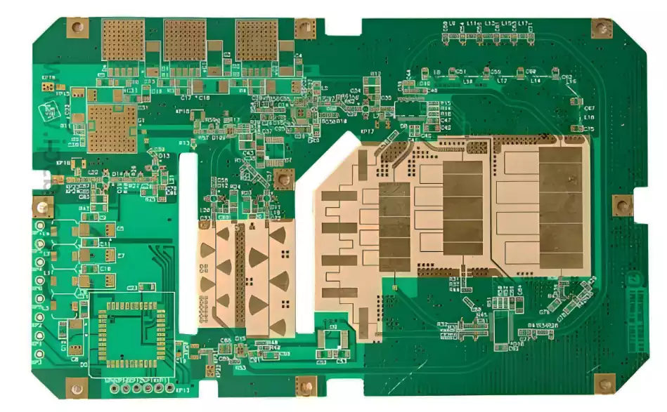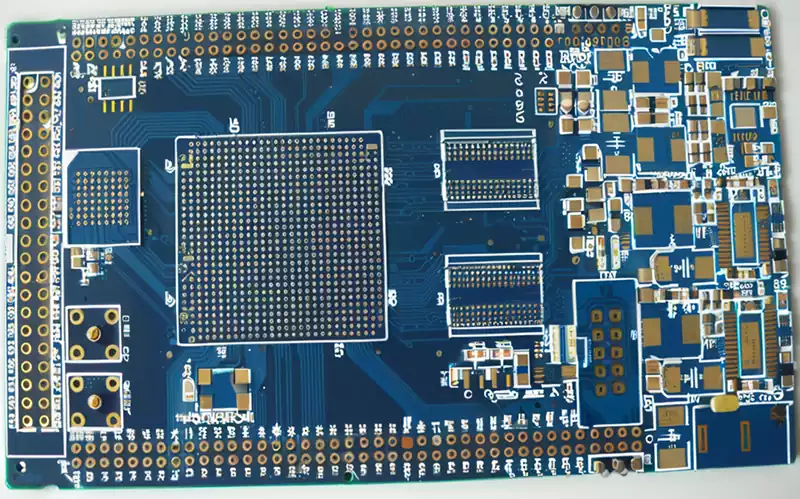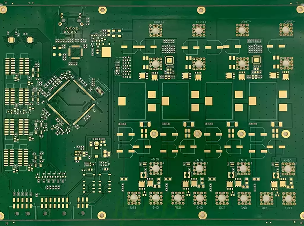
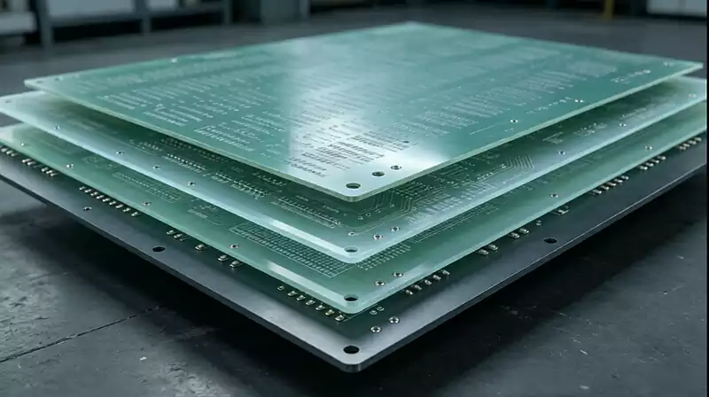
A heavy copper pcb multilayer board combines increased copper thickness with multiple conductive layers to support demanding electrical and thermal requirements. Unlike conventional PCBs designed mainly for low- to moderate-current circuits, this structure is intended for applications that require higher current capacity, improved heat distribution, and complex electrical connections within a limited space. By integrating thicker copper layers into a multilayer construction, designers can develop compact circuit boards capable of handling substantial power loads.
Heavy copper PCBs typically use thicker copper than standard circuit boards, although the exact thickness depends on the design and manufacturing specification. Multilayer construction adds another level of flexibility by allowing power, ground, control, and signal circuits to occupy separate layers. This arrangement helps manage current distribution while reducing the need for large external wiring structures.
The combination is particularly useful when a product contains high-current power sections alongside sensitive control or communication circuits. However, achieving the expected performance requires careful coordination of copper thickness, layer arrangement, dielectric materials, and thermal design.
Copper Thickness and Multilayer Stackup Design
Copper thickness is one of the most important parameters in a heavy copper PCB. Thicker copper can reduce conductor resistance and help carry higher current, but it also affects trace geometry, etching accuracy, and the overall fabrication process. Designers must determine the required copper weight according to current demand, allowable temperature rise, conductor width, and available board space.
In a multilayer design, copper thickness does not need to be identical across every layer. Power layers may require heavier copper to handle large currents, while signal layers can use thinner copper to maintain routing precision. This selective arrangement helps balance electrical performance with manufacturing complexity.
The layer stackup should also provide suitable separation between high-current circuits and sensitive signal paths. Ground planes can offer stable reference paths and help control electromagnetic interference, while dedicated power planes support more consistent power distribution. The position of each layer should be considered together with the direction of current flow and the return-current paths.
Dielectric thickness and material selection are equally important. The insulating layers must provide sufficient electrical isolation while maintaining appropriate thermal and mechanical properties. In high-power applications, materials with suitable thermal performance can help transfer heat away from copper conductors and reduce localized temperature increases.
Electrical and Thermal Management in Heavy Copper PCB Multilayer Board Design
High-current operation generates heat through conductor resistance, component losses, and power conversion activity. Although thicker copper can reduce resistance and improve heat spreading, it does not eliminate the need for a complete thermal management strategy. Designers should evaluate the expected current distribution, operating temperature, ambient conditions, and heat sources across the entire board.
Wide copper traces and planes can reduce current density and distribute heat over a larger area. Where current must move between layers, appropriately designed vias or other conductive structures are necessary. Via quantity, diameter, plating thickness, and placement should be evaluated according to the current they need to carry and the thermal requirements of the board.
Thermal vias can help transfer heat between layers, especially beneath power components and other concentrated heat sources. However, their effectiveness depends on the surrounding copper structure, board materials, and connection to external heat-dissipation features. Designers should avoid assuming that adding vias alone will solve thermal problems.
Electrical spacing must also be maintained. High-current circuits may involve substantial voltage differences, so clearance, creepage distance, insulation thickness, and operating voltage need to be considered. These requirements are especially important in power conversion equipment and industrial control systems, where electrical safety and long-term reliability are essential.
Manufacturing Challenges of Heavy Copper Multilayer Boards
Manufacturing a heavy copper multilayer board requires tighter coordination between material preparation, inner-layer processing, lamination, drilling, plating, and final circuit formation. Thick copper can make fine-line etching more difficult because the etching process must remove more material while preserving the intended conductor geometry. As copper thickness increases, designers may need wider traces and larger spacing to maintain manufacturability.
Lamination is another important consideration. Different copper thicknesses and circuit densities can create variations in the stackup, affecting resin flow and insulation uniformity. The PCB manufacturer must select appropriate prepreg materials and lamination parameters to achieve reliable bonding between layers.
Drilling and via plating also require careful process control. Thick copper structures and multilayer connections can increase the difficulty of producing consistent plated-through holes. Hole-wall copper thickness, via reliability, and interlayer connectivity should be verified through suitable inspection and testing procedures.
Quality control should cover more than basic electrical continuity. Cross-sectional analysis can help evaluate layer alignment, copper thickness, dielectric distribution, and via plating quality. Electrical testing and thermal evaluation can further confirm whether the finished board meets its design requirements.
Applications of Heavy Copper PCB Multilayer Board Technology
Heavy copper pcb multilayer boards are used in electronic systems that combine high power density with complex circuit functionality. Industrial power supplies and converters are common examples because they require reliable current paths and effective heat distribution. In these products, dedicated power layers can carry substantial current while other layers support control and monitoring circuits.
Renewable energy equipment, including solar power conversion systems and energy storage devices, may also benefit from this construction. These systems often involve high-current connections, power switching, and demanding operating conditions. A properly designed multilayer structure can help integrate these functions while controlling electrical and thermal performance.
Electric vehicle charging equipment, motor drives, welding systems, and industrial automation devices are other potential applications. Their circuit boards may need to accommodate high current, switching noise, and compact mechanical layouts. The appropriate copper thickness and layer count depend on the actual electrical load and system architecture.
A heavy copper PCB multilayer board is not automatically the best solution for every high-power product. The additional copper and more complex fabrication processes can increase cost and design constraints. Engineers should compare the benefits against alternatives such as busbars, separate power modules, or conventional multilayer PCBs with optimized conductor dimensions.
Choosing a Heavy Copper PCB Multilayer Board Manufacturer
Selecting a suitable manufacturing partner is important because heavy copper multilayer fabrication involves more than simply increasing copper weight. The manufacturer should be able to evaluate the proposed stackup, trace geometry, material selection, drilling requirements, and lamination process before production.
Designers should provide clear information about maximum current, operating voltage, temperature limits, layer count, copper thickness, and component placement. These details help the manufacturing team assess whether the design is practical and identify potential risks before fabrication begins.
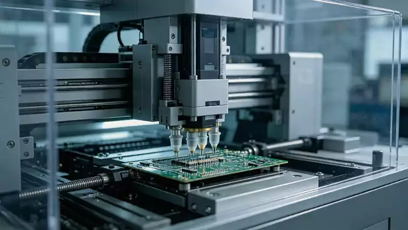
iPCB provides PCB manufacturing and assembly services for projects involving multilayer structures, high-current circuits, and demanding electronic applications. Integrating design review, fabrication process planning, and assembly requirements can help improve manufacturability and maintain consistent production quality.
A successful heavy copper pcb multilayer board depends on the relationship between electrical design, thermal management, material selection, and manufacturing control. When these factors are addressed together, the resulting PCB can provide a reliable foundation for compact, high-power electronic systems.