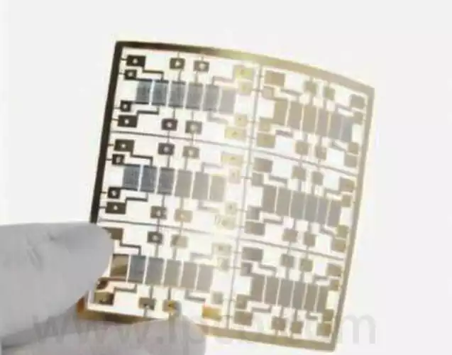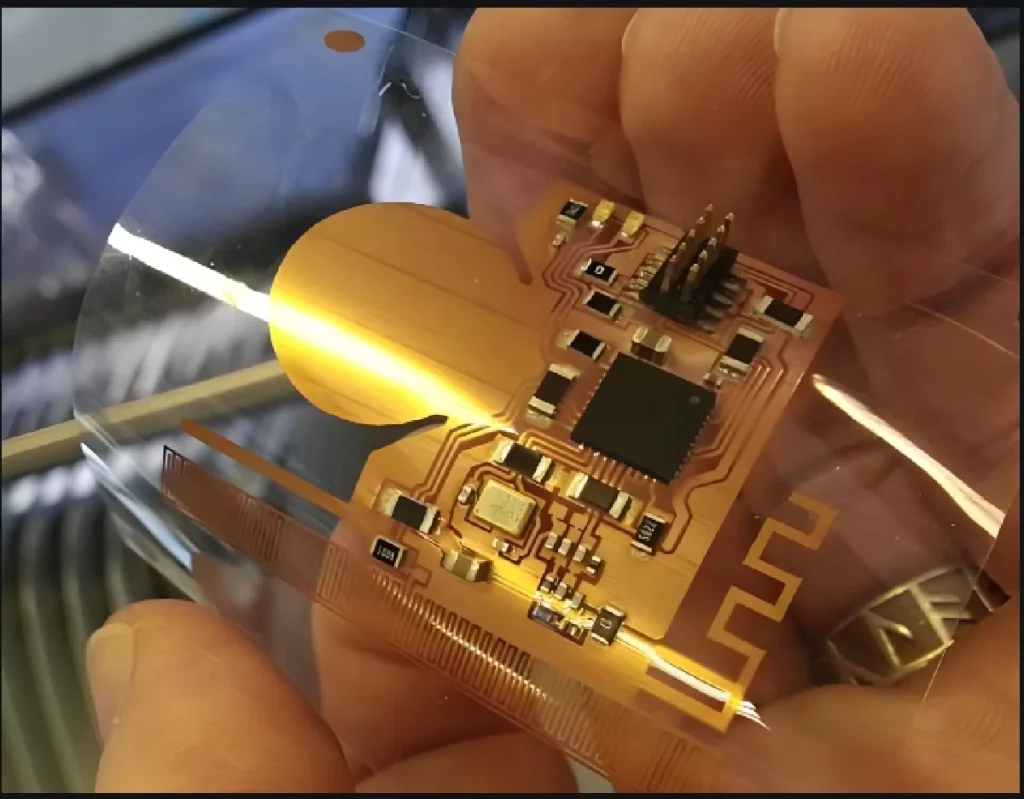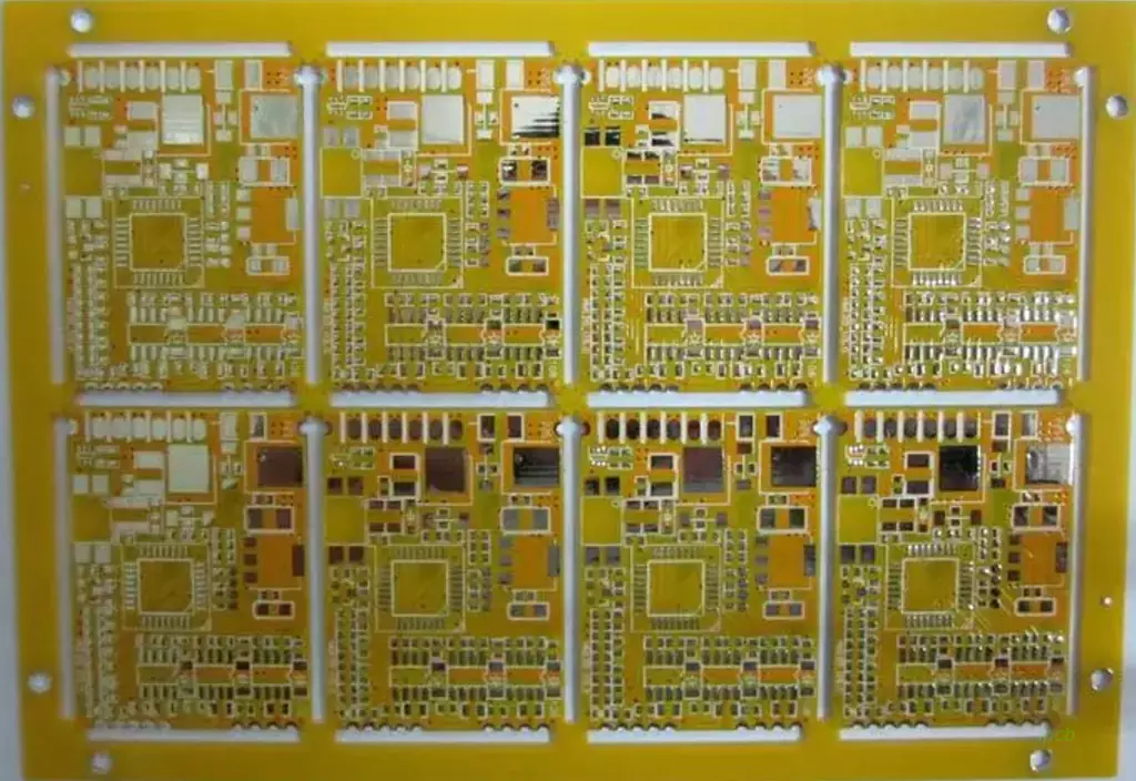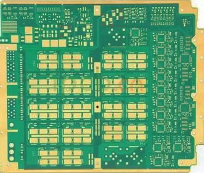
OSP PCB surface finish is a widely used surface treatment that protects exposed copper on printed circuit boards and helps maintain solderability during electronic assembly. OSP stands for Organic Solderability Preservative, a chemical coating applied to exposed copper surfaces to reduce oxidation before components are soldered onto the board. Unlike metallic finishes such as ENIG or immersion silver, OSP does not create a thick metal layer. Instead, it forms a thin organic protective film that helps preserve the condition of copper pads during PCB storage, handling, and manufacturing.
The condition of exposed copper directly affects solder joint formation. When copper oxidizes, solder may not wet the pad evenly, increasing the risk of poor connections and assembly defects. OSP addresses this issue through a controlled chemical process that deposits a protective layer without significantly changing the dimensions of the copper features. Its relatively simple structure, flat surface, and compatibility with common PCB assembly processes make it suitable for many consumer, industrial, and electronic control applications. However, its performance depends on coating quality, storage conditions, handling practices, and the number of thermal processes involved.
How OSP PCB Surface Finish Protects Copper
The primary function of OSP is to protect exposed copper from oxidation while keeping the surface suitable for soldering. During the treatment process, the PCB undergoes cleaning and micro-etching to remove contaminants and prepare the copper surface. It is then immersed in an OSP chemical solution, where organic molecules form a thin protective film on the exposed copper.
This film acts as a barrier between copper and the surrounding environment. By limiting direct exposure to oxygen and moisture, it slows the formation of copper oxides that can interfere with solder wetting. When the PCB enters the soldering process, the protective organic layer is removed or decomposed under the appropriate thermal conditions, allowing solder to contact the underlying copper.
One important characteristic of OSP is that it maintains a relatively flat surface. Because the coating is extremely thin, it does not create the noticeable surface-height differences that may occur with some metallic finishes. This can be beneficial for fine-pitch surface-mount components, including packages with closely spaced terminals, where consistent pad geometry supports accurate component placement and solder paste printing.
The coating also preserves the underlying copper dimensions. This is useful for designs with fine traces and closely spaced pads because the surface treatment does not require a substantial metal deposition layer. Nevertheless, the final solderability still depends on the condition of the copper, the quality of the OSP film, and the PCB’s handling and storage history.
OSP PCB Surface Finish Manufacturing Process
The quality of an OSP finish begins with copper surface preparation. Before the organic coating is applied, the exposed copper must be free from oxidation, oils, fingerprints, and other contaminants. Cleaning removes unwanted residues, while micro-etching removes a controlled amount of copper to expose a fresh surface. If preparation is inconsistent, the protective film may form unevenly and produce differences in solderability across the board.
After preparation, the PCB enters the OSP treatment bath. The organic molecules react with the copper surface and form a thin protective layer. Process parameters such as solution concentration, temperature, immersion time, and bath condition influence coating formation. Manufacturers must control these variables to achieve consistent coverage and avoid defects caused by contamination or unsuitable chemical conditions.
Rinsing and drying follow the coating process. These steps help remove residual chemicals and prepare the boards for subsequent inspection, packaging, or assembly. The finished surface should be uniform, clean, and free from visible contamination. Since the coating is very thin, visual appearance alone cannot fully establish its protective performance. Process monitoring and appropriate quality checks are therefore important.
After treatment, storage and packaging become critical. OSP coatings are more sensitive to handling and environmental exposure than some metallic surface finishes. Fingerprints, moisture, prolonged storage, and unsuitable packaging conditions can reduce solderability. Manufacturers and customers should follow the specified storage requirements and avoid unnecessary contact with exposed pads. The recommended shelf life depends on the OSP chemistry, process control, packaging, and storage environment rather than a single universal period.
Advantages and Limitations of OSP PCB Surface Finish
One major advantage of OSP is its relatively flat surface. This characteristic supports fine-pitch component assembly and helps maintain consistent contact geometry between solder paste and PCB pads. It can also simplify the fabrication process because the coating does not involve depositing a relatively thick metallic layer.
OSP is also attractive because it does not require precious metals such as gold or silver. Its material and processing costs can therefore be favorable for applications where the design does not require the additional properties of a metallic finish. The process is compatible with common lead-free and leaded soldering systems when the coating and assembly conditions are properly matched.
However, OSP has limitations that should be considered during surface finish selection. Its protective film is relatively sensitive to physical handling, contamination, and environmental exposure. Repeated thermal processing can also affect the coating and the condition of the exposed copper. For boards that require multiple soldering operations, the assembly sequence and thermal history need careful evaluation to ensure that solderability remains acceptable.
OSP also does not provide the same corrosion resistance or contact characteristics as certain metallic finishes. For example, applications requiring exposed contacts for repeated electrical connection may need a different surface treatment. Likewise, boards intended for long storage periods or demanding environmental conditions may require a finish with more suitable protection and durability.
Another consideration is that OSP does not create a conductive protective metal layer over the copper. Its purpose is to preserve copper solderability, not to provide a wear-resistant contact surface. The finish should therefore be selected according to the actual function of the exposed pads rather than treated as a universal solution for every PCB design.
Choosing OSP PCB Surface Finish for PCB Applications
OSP is often suitable for electronic products that use conventional soldered connections and require a flat, cost-conscious surface finish. It can be used in many consumer electronics, communication devices, industrial control boards, and other assemblies where exposed copper pads are primarily intended for soldering.
The selection process should begin with the PCB’s assembly requirements. Engineers need to consider component package types, soldering methods, the number of reflow or wave-soldering operations, and the time between PCB fabrication and assembly. If a board includes fine-pitch components, the flatness of OSP may offer practical benefits. If the design includes exposed contact fingers, repeated mating connections, or unusually demanding storage conditions, another surface finish may be more appropriate.
Manufacturing capability is equally important. Consistent copper preparation, controlled chemical treatment, suitable packaging, and clear shelf-life management all influence the reliability of OSP coated boards. The PCB fabricator and assembly manufacturer should coordinate their process requirements so that the finish remains in an acceptable condition until soldering is completed.
Ultimately, osp pcb surface finish provides a practical way to protect exposed copper while preserving the flat pad geometry needed for reliable soldering. Its advantages include a thin protective coating, favorable cost characteristics, and compatibility with many standard PCB assembly processes. Its limitations, particularly sensitivity to handling, storage, and repeated thermal exposure, must also be considered. Selecting OSP based on the board’s electrical design, assembly sequence, and expected service conditions helps achieve consistent manufacturing quality and dependable solder joints.