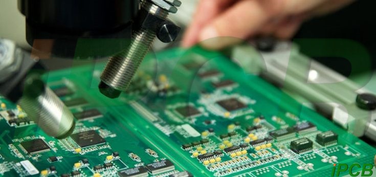
In the printed circuit board industry, the OSP process is widely used. Thanks to its outstanding advantages—including low cost, a simple manufacturing process and excellent solder joint reliability—it has become the preferred process for many PCB manufacturers.
OSP, or Organic Solderable Protective Coating, involves the chemical deposition of a thin organic protective film onto the surface of clean, uncontaminated bare copper pads. This film possesses excellent anti-oxidation properties and thermal shock resistance, effectively isolating the copper surface from contaminants such as air and moisture prior to soldering, thereby preventing oxidation and degradation.
It should be noted that this organic film serves as a temporary protective layer. During the subsequent soldering process, it is completely decomposed and removed by the action of flux and the high temperatures involved, allowing the molten solder to come into direct contact with and bond to the bare copper surface. This results in strong, high-quality solder joints, ensuring the electrical connectivity of the PCB.
Advantages and Disadvantages of OSP PCB
Advantages
Significant cost advantages: compared to other surface treatment processes, the OSP process involves lower raw material and manufacturing costs, enabling effective control of overall PCB production costs.
The pad surface is highly flat, with no unevenness, making it suitable for the mounting of fine-pitch components and capable of meeting the production requirements of high-precision PCBs.
High solder joint reliability: as the solder bonds directly to the pure copper pad, the influence of intermediate transition layers is avoided, resulting in greater connection stability.
The process is environmentally friendly and non-polluting: no harmful heavy metals such as lead are used throughout the process, complying with the environmental standards and development trends of the modern electronics industry.
Disadvantages
The organic protective film is relatively thin and lacks sufficient physical strength; it is highly susceptible to scratches and contamination during storage and handling, thereby losing its protective function.
It is extremely sensitive to moisture and oxygen in the environment; improper storage conditions can easily lead to film degradation and oxidation of the copper surface, resulting in a relatively short shelf life.
Heat resistance is limited; it cannot withstand multiple reflow soldering cycles. The industry generally recommends no more than 2–3 reflow cycles, as exceeding this may affect solderability.
Visual inspection of solder joints is challenging; after soldering, the pads are completely covered by solder and do not exhibit the distinct reflectivity seen on tin-plated boards, making it difficult to assess joint quality at a glance.
During SMT placement, reflow soldering and subsequent assembly, OSP PCBs require greater care and attention. Operators must exercise extreme caution and strictly adhere to operational guidelines to prevent board failure caused by improper handling.
1.Pre-opening inspection
Check the integrity of the packaging to ensure the vacuum-sealed packaging is undamaged and free from leaks. If the packaging is damaged, assess immediately whether the boards have oxidised.
Check the humidity indicator card inside the packaging bag to confirm that the colour is within the safe range (typically blue); if the indicator card shows moisture (e.g. turning pink), investigate the cause immediately and assess the risk to the boards’ solderability.
2.Handling and Operating Procedures
Clean, lint-free gloves must be worn during handling to prevent contaminants such as sweat or oils from coming into contact with the pads and damaging the OSP protective film.
When handling, touch only the edges of the PCB; do not touch the surface of the OSP pads directly with fingers or other objects to avoid scratching or contaminating the film.
During handling, avoid dragging the PCB across flat surfaces and prevent the board from rubbing against other hard objects to avoid scratching the OSP film and compromising its protective function.
3.Printing and Placement Process
Solder paste printing: There are no special operational requirements; simply follow standard SMT procedures to ensure uniform solder paste printing with no missed areas or bridging.
Component Placement: Follow standard placement procedures, paying particular attention to placement pressure. Pressure should not be excessive to avoid mechanical damage to the pads and damage to the OSP film.
4.Key Points for Reflow Soldering
Reflow soldering is a critical stage for removing the OSP film and forming effective solder joints. Parameters for each temperature zone must be strictly controlled to ensure soldering quality.
Preheating Zone: Control the heating rate to avoid excessive heating, as this may cause the OSP film to spatter due to heat, resulting in solder balls and other soldering defects.
Active Zone/Reflow Zone: Ensure adequate hot air convection to guarantee that the flux can uniformly and thoroughly remove the OSP film from all pad surfaces; simultaneously, the peak temperature must reach the specified standard to ensure the solder is fully melted and wets the bare copper pads effectively.
Post-reflow inspection: Upon completion of soldering, the quality of the solder joints must be inspected promptly. Qualified solder joints should appear bright and smooth, with the solder completely covering the pad; if issues such as solder rejection, solder balling or excessive wetting angles occur, it is highly likely that the OSP film has not been completely removed or that the copper surface has oxidised, requiring immediate investigation and rectification.
5.Rework and Repair Guidelines
Limit the number of rework operations: It is not recommended to perform more than 1–2 rework operations on the same solder joint, as each heating cycle depletes the OSP coating and accelerates oxidation of the copper surface, thereby compromising the reliability of the joint.
Add fresh flux: When reworking, apply an appropriate amount of fresh flux to aid in removing the damaged OSP coating and prevent secondary oxidation of the copper surface.
Selection of Suitable Soldering Tips: Select soldering tips of appropriate shape and size based on the size and location of the solder joint to avoid prolonged heating of the pad, thereby minimising damage to the OSP film and copper surface.
6.Considerations for Subsequent Processes
Wave Soldering Adaptation: If OSP pcbs are to undergo wave soldering, a highly active flux must be used to ensure that the copper surfaces within the through-hole components are adequately wetted by the solder, thereby guaranteeing soldering quality.
Test point treatment: If the PCB contains OSP pads for testing, repeated reflow soldering may cause surface oxidation, leading to poor contact during testing. It is recommended to apply a hard surface treatment, such as gold plating, to critical test points to enhance their resistance to oxidation and improve contact reliability.
Applications of OSP PCBs
Consumer electronics industry: This sector encompasses smartphones, tablets, smart wearable devices, laptops and control boards for household appliances. OSP PCBs are suitable for fine-pitch components (such as BGA and QFP packages) and meet the cost control requirements of high-volume production, making them one of the preferred solutions for consumer electronics PCBs.
Automotive Electronics Industry: Suitable for in-vehicle navigation systems, ADAS (Advanced Driver Assistance Systems), and battery management systems. Utilising OSP formulations with excellent temperature resistance, these boards can withstand wide temperature ranges and multiple reflow soldering cycles, meeting the long-term reliability requirements of automotive electronics. They must pass relevant certifications such as AEC-Q200.
Medical device industry: Used in equipment such as ECG monitors, ultrasound diagnostic devices and infusion pumps. Utilising medical-grade OSP agents that comply with the ISO 10993 biocompatibility standard, these solutions are non-toxic and feature high cleanliness, and can withstand wiping with common medical disinfectants.
Industrial Control Sector: Suitable for PLCs (Programmable Logic Controllers), variable frequency drives, sensors and similar equipment. It withstands high-temperature, high-humidity and dusty factory workshop environments, meeting the requirements for long-term stable operation and extended storage periods.
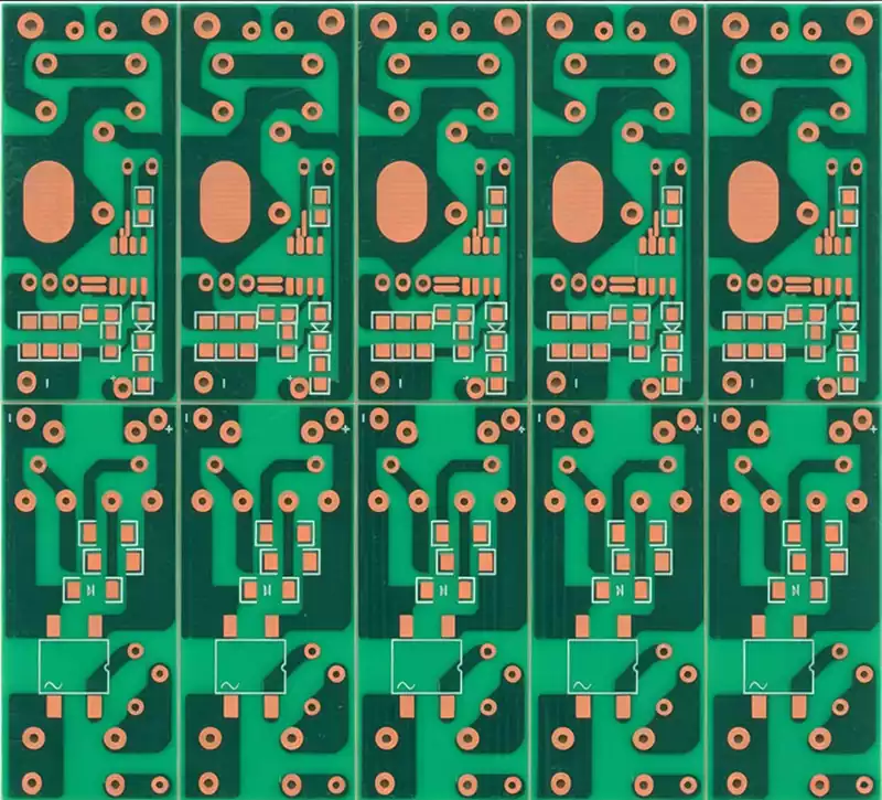
General Electronics Sector: Includes computer motherboards, memory modules, standard general-purpose circuit boards and similar products. As there are no requirements for long-term storage or wear-resistant plugging and unplugging, the cost-effectiveness of the OSP process can be fully utilised to reduce production costs.
The OSP process combines cost-effectiveness with reliability and offers excellent prospects for future applications. Provided that operating procedures are strictly adhered to and storage and process conditions are carefully controlled, its advantages can be fully utilised to meet the soldering requirements of a wide range of electronic products.