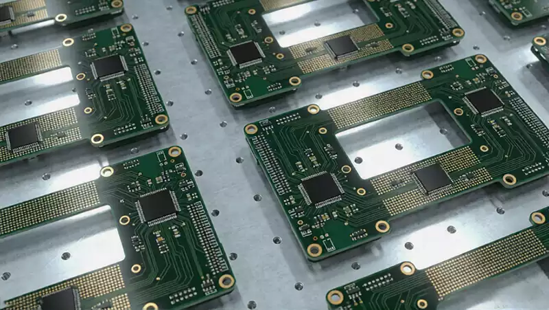
SMT soldering quality is the foundation of electronic assembly reliability. Starting from the appearance criteria of high-quality solder joints, this article systematically analyzes the causes of typical defects such as tombstoning, solder balls, and solder bridging, and provides corresponding process control measures to offer practical guidance for on-site quality improvement.
Appearance Standards for High-Quality Soldering Joints
Qualified SMT soldering joints must meet consistent appearance and performance standards. The solder should exhibit excellent wettability, with a continuous and uniform distribution across the pad surface. The solder layer should gradually taper toward the edges, and the contact angle should be less than 30°. Small pads should form a smooth concave meniscus.
The soldered area must be free of oxides, contaminants, and other impurities. The solder volume should be appropriate, without excessive accumulation or insufficient coverage. Component terminations and leads should be accurately centered on the pads without offset or overhang. The solder joint surface should be smooth, bright, flat, and uniformly formed, with no pits, bumps, burrs, or other defects. These criteria apply to all soldering processes and PCB locations.
Common Soldering Defects: Causes and Solutions
1.Tombstoning
Tombstoning refers to a defect in which one end of a chip component lifts from the PCB and stands upright. The root cause is an imbalance in the solder wetting forces acting on the two ends of the component, resulting in uneven torque during reflow.
Specific causes include four major categories:
Poor pad design or excessive temperature differences across the PCB, leading to uneven heat absorption between pads. This can be addressed by optimizing pad geometry and PCB layout.
Insufficient solder paste activity, improper printing parameters, or incorrect stencil aperture dimensions. High-activity solder paste and optimized printing processes should be adopted.
Uneven Z-axis placement force or component misalignment during pick-and-place operations. Placement machine parameters should be calibrated accordingly.
Improper reflow temperature profiles or excessive board temperature differentials. Product-specific temperature profiles should be developed and optimized.
In addition, during nitrogen reflow soldering, the oxygen concentration should be precisely controlled at approximately 100 ppm. Excessively low oxygen levels may increase the occurrence of tombstoning defects.
2.Solder Ball Formation
The appearance of scattered solder balls on the PCB after soldering is a common issue caused by multiple process-related abnormalities.
From a material perspective, low metal content in the solder paste, excessive flux content, moisture absorption, oxidation, or deterioration caused by repeated use after opening can significantly increase the likelihood of solder ball formation.
From a process and equipment perspective, an excessively steep heating rate during reflow or insufficient preheating may prevent complete solvent evaporation. Printing misalignment, inadequate production cleanliness, or improper Z-axis placement parameters may cause solder paste to be squeezed outside the pad area. Chemically etched stencils with poor aperture precision or insufficient thickness may also lead to excessive solder paste deposition and overflow.
To prevent this defect, manufacturers should optimize the reflow preheating profile, use fresh and qualified solder paste, accurately calibrate printing and placement equipment, and select stencil specifications that match the required assembly precision.
3.Solder Mask Blistering
The fundamental cause of PCB solder mask blistering is the expansion of residual moisture and trapped gases inside the PCB during high-temperature soldering, which causes delamination between the solder mask and the substrate. This defect is most commonly observed around pad areas.
To effectively prevent solder mask blistering, a comprehensive PCB material control system should be implemented:
All incoming PCBs must undergo quality inspection before storage.
PCBs should be stored in a dry and well-ventilated environment.
Storage duration should not exceed six months.
Before assembly, PCBs should be baked at 105°C for 4–6 hours to completely remove absorbed moisture.
Wave soldering preheat parameters should be strictly controlled.
For standard PCB materials, the preheat temperature should generally be maintained between 100°C and 120°C. When water-based fluxes are used, the preheat temperature should be increased to 110°C–125°C to ensure complete evaporation of moisture from both the PCB and flux, thereby preventing blistering during soldering.
4.Wicking
Wicking is a defect commonly associated with vapor-phase reflow soldering. It occurs when molten solder migrates away from the effective pad area and travels upward along the component leads toward the package body, resulting in hidden insufficient solder joints that can severely affect electrical reliability.
The primary causes include:
Inadequate PCB preheating.
Poor pad solderability.
Poor lead coplanarity.
Corresponding corrective measures include:
Thoroughly preheating the PCB before soldering to achieve uniform board temperature.
Verifying pad plating quality and solderability in advance and rejecting defective boards.
Selecting components with acceptable lead flatness and coplanarity.
These measures help eliminate wicking issues from both material and process perspectives.
5.Cracking of Chip Components
Miniature chip components, particularly multilayer ceramic capacitors (MLCCs), are highly susceptible to cracking during manufacturing. The primary causes are thermal shock and mechanical stress.
Several preventive measures can be implemented:
Optimize the reflow temperature profile by extending the preheat stage and reducing the heating rate to minimize temperature differentials between components and the PCB.
Precisely adjust pick-and-place machine Z-axis travel and placement force settings to avoid excessive mechanical stress.
Improve depanelization tooling and blade sharpness.
Correct PCB warpage and deformation to reduce tensile stress caused by board flexing.
These measures help protect component integrity throughout the assembly process.
6.Dull Solder Joints and Excessive Residue
Poor solder joint appearance and excessive flux residue are common SMT quality concerns.
The main causes include:
Lack of timely forced-air cooling after reflow soldering, resulting in an insufficient cooling rate.
Low metal content and excessive flux content in the solder paste, preventing complete volatilization during reflow.
To address these issues:
Introduce forced-air cooling after soldering.
Use high-quality solder paste with higher metal content and low-residue formulations.
Fine-tune the high-temperature soak stage to ensure complete flux volatilization.
These measures effectively improve solder joint brightness and reduce surface residue.
7.PCB Warpage and Distortion
PCB warpage and distortion can directly cause component misalignment, insufficient solder joints, solder bridging, and other secondary quality defects, significantly affecting production yield.
Common preventive and corrective measures include:
Selecting PCB materials with a high glass transition temperature (High-Tg).
Increasing board thickness where appropriate.
Optimizing board aspect ratios.
Balancing copper distribution on both sides of the PCB.
Adding copper mesh patterns in unused areas to improve rigidity and thermal balance.
Baking PCBs at 105°C for four hours before assembly to relieve internal stress.
Properly adjusting fixture spacing to accommodate thermal expansion.
Reducing peak soldering temperatures where process specifications allow.
For slightly warped boards, thermal fixtures may be used to eliminate residual stress and restore flatness.
8.Solder Bridging
Lead bridging is a common defect in the soldering of fine-pitch components and occurs when solder unintentionally connects adjacent leads, resulting in an electrical short circuit.
The causes span materials, equipment, and process factors:
Solder paste with excessively high metal content, low viscosity, or poor slump resistance may spread beyond the leads after preheating.
Insufficient printing alignment accuracy, improper stencil aperture design, or uneven PCB pad plating thickness can cause excessive and misaligned solder paste deposition.
Improper Z-axis placement settings and excessively rapid reflow preheating may cause solvents to evaporate suddenly, promoting solder flow and bridging.
To prevent solder bridging, manufacturers should select solder paste appropriate for the application, calibrate printing alignment accuracy, optimize stencil and pad designs, and fine-tune placement and reflow parameters.
9.Other Common Soldering Defects
In addition to the defects discussed above, SMT production may encounter several other common soldering issues, including poor wettability, insufficient solder fill, lead damage, and localized solder paste omission.
Poor solder wetting and inadequate solderability are commonly caused by oxidized or contaminated component leads, poor solder paste quality, or excessive reflow temperatures, often resulting in hidden cold solder joints.
Insufficient solder fill and inadequate solder joint volume are typically caused by undersized stencil apertures, improperly matched reflow profiles, or low metal content in the solder paste.
Lead deformation frequently occurs during transportation, handling, or manual assembly operations. In addition, poor lead coplanarity can directly affect solder joint formation quality.
Localized solder paste omission and interrupted deposits are often observed during first-article production or after equipment restart. The primary causes include process parameter fluctuations and clogged stencil apertures that have not been properly cleaned.
The prevention and control of SMT soldering defects must encompass the entire manufacturing chain, including materials, equipment, and process management. Success depends on proactive prevention and the coordinated optimization of process parameters.
Manufacturers should adhere to standardized inspection procedures, perform meticulous process adjustments, and continuously monitor critical process variables. Only through comprehensive process control can defect rates be effectively reduced while ensuring consistent and stable SMT soldering quality.