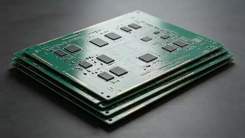
High layer count pcb, known in the industry as HLC (High Layer Count), are defined as through-hole printed circuit boards with six or more layers. With PCB manufacturing processes continuously evolving, boards exceeding 40 layers have now reached mass production and widespread market adoption — no longer a niche, high-end product.
Thanks to their complex layer structures, stable electrical performance, and process characteristics suited to high-end equipment, high layer count pcbs are widely used across various cutting-edge fields. Core application scenarios include file servers, data storage terminals, GPS positioning devices, satellite communication systems, high-performance computing servers, meteorological monitoring and analysis instruments, precision medical equipment, aerospace systems, industrial automation control systems, and military electronics. In most high-end applications, high layer count pcb must be paired with high-frequency, high-speed, and other specialty materials to meet the demands of high-frequency transmission, low loss, and high stability.
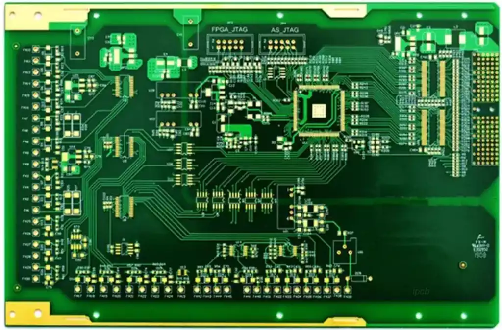
Core Characteristics of high layer count pcb
1.Layer Count: The mainstream high layer count pcb on the market today generally feature 12 layers or more. Ultra-high-end products can exceed 40 layers, accommodating the complex routing requirements of high-end equipment.
2.Board Thickness: The overall board thickness is no less than 0.8 mm. Common industry-standard thicknesses include 1.0 mm, 1.2 mm, 1.6 mm, and 2.0 mm. Thickness can be customized based on equipment load-bearing, insulation, and EMI requirements.
3.Surface Copper Thickness: The base copper layer is typically 0.5 oz or 1 oz. After electroplating, the overall copper thickness on the board surface is at least 1 oz, ensuring stable conductivity and current-carrying capacity.
4.Finished Board Size: Unlike standard small PCBs, high layer count pcb are generally larger in size, making them especially suitable for servers and large-scale communication equipment. Industry oversized high layer count pcb can exceed 0.5 meters. Cases have been recorded with panels as large as 24 × 30 inches (approximately 610 × 762 mm), where a single panel yields only one finished board.
5.Specialty Process Configuration: To meet high-precision, high-reliability application requirements, high layer count pcb universally employ customized specialty processes. Core processes include various via-filling techniques, press-fit forming, controlled-depth drilling, and board-edge plating — all designed to maximize product performance.
Key Production Processes for high layer count pcb
1.Via-Filling Process
Via filling is one of the core processes in high layer count pcb production. Depending on material and method, it is divided into four types: solder mask via filling, resin via filling, conductive adhesive via filling, and electroplated via filling. The primary purpose is to resolve insulation, connectivity, and planarity issues in high-density routing, preventing short circuits and signal interference. Among these, resin via filling combined with electroplated planarization (VIP/POFV) has become the standard configuration for high-end high layer count pcb.
2.Press-Fit Process
This is a solderless mechanical connection technology. Component leads are pressed into plated through-holes (PTH) using mechanical force, relying on a precision interference fit between the hole wall and the lead to achieve both electrical connectivity and mechanical fixation. No high-temperature soldering is required, eliminating thermal damage. The process demands extremely high aperture accuracy, with tolerances strictly controlled within ±0.05 mm. The “fish-eye” terminal structure undergoes elastic deformation during insertion, creating a tight fit against the hole wall that delivers low contact impedance and high vibration resistance. It is widely used in automotive electronics, communication equipment, and industrial automation.
3.Controlled-Depth Drilling Process
Controlled-depth drilling is a non-through drilling method that penetrates the board only to a specified depth according to the design, rather than drilling through the entire board. This process is primarily used for layer-to-layer connectivity or layer-to-layer insulation in multilayer boards, meeting the special routing layout requirements of precision equipment.
4.Board-Edge Plating Process
This process metallizes (primarily copper-plates) the outer edges of the PCB. It can be applied to one side, both sides, or all edges. It effectively improves the continuity and stability of edge electrical connections while enhancing the board’s mechanical strength, bend resistance, and wear resistance. It is especially suited for aerospace, high-end servers, and other scenarios with extremely high reliability requirements.
Industry Development History
In the early 2000s, China’s HLC industry was still in its infancy. Products were concentrated at 6–12 layers, with limited process precision: line width/spacing was 100/100 μm, the minimum mechanical drill diameter was 300 μm, and the minimum annular ring width was 100 μm. At that time, products were mainly used in communication servers, computer motherboards, memory modules, and graphics cards. Some high-end products had already begun experimenting with mechanical blind and buried via processes, with the 12-layer high-end memory module PCB being a typical example.
Since then, through continuous breakthroughs in core processes such as electroplated through-hole processing, lamination uniformity, mechanical drilling precision, and dimensional compensation, HLC’s overall manufacturing capability has risen sharply. Today, every metric — layer count, board thickness, routing fineness, minimum aperture precision, and dimensional stability — has seen leapfrog improvements, fully supporting the manufacturing demands of ultra-high-density, ultra-precision, and high-reliability equipment.
Core Manufacturing Challenges of high layer count pcb
Inter-Layer Registration Accuracy Is Difficult to Control
The more layers a board has, the more significant the cumulative registration error becomes. High-end high layer count pcb require inter-layer registration accuracy within ±75 μm. For large-format boards, temperature and humidity fluctuations, as well as CTE differences between core boards from different batches, make inter-layer shift and misalignment highly likely — making precise registration extremely challenging.
Inner Layer Production Yield Is Relatively Low
High-end high layer count pcb often use specialty materials such as high-Tg, high-speed/high-frequency, thick-copper, and thin-dielectric laminates. The requirements for pattern transfer and dimensional accuracy far exceed those of standard boards. At the same time, ultra-fine line widths/spacings and annular ring designs are prone to plating non-uniformity, opens, shorts, and micro-shorts. Thin core boards are also susceptible to wrinkling and warping, causing exposure misalignment and pattern distortion. Combined with the large board size, scrap costs are extremely high.
Lamination Process Carries High Defect Risk
With many layers of core boards and prepreg (PP) sheets stacked together, the lamination process is prone to slippage, delamination, resin voids, and bubbles. The process must balance multiple parameters simultaneously: heat resistance, pressure resistance, resin content, and dielectric layer uniformity. As layer count increases, the board’s expansion and contraction behavior becomes more complex, making dimensional compensation far more difficult. Thin insulation layer structures also tend to cause insulation failures and reliability test non-compliance.
Drilling Process Is Highly Demanding
Specialty materials such as high-Tg, high-frequency, and thick-copper laminates are hard and wear-resistant. Drilling these materials often produces rough hole walls and burrs at the hole entrance, making subsequent desmearing and hole wall activation more difficult. Thick boards and accumulated copper thickness accelerate drill bit wear and increase the risk of breakage. In dense BGA areas, the extremely small spacing between vias creates a risk of CAF (Conductive Anode Filament) migration over long-term use, which can lead to leakage or short-circuit failures.
Key Process Control Points for high layer count pcb
Precision Material Selection: Prioritize high-performance copper-clad laminates with low dielectric constant (Low DK), low coefficient of thermal expansion (Low CTE), and low moisture absorption. This prevents warping, signal loss, and moisture-induced leakage at the source, ensuring process compatibility and long-term operational stability.
Optimized Stack-Up Design: Scientifically combine core boards and prepreg sheets based on voltage withstand, heat resistance, and insulation requirements. Reasonably configure dielectric layer thickness and resin content to ensure balanced mechanical strength, heat dissipation, and insulation performance across the stack-up. When no special requirements exist, use the same brand and batch of materials throughout to minimize deformation and registration errors caused by material variation.
Upgraded Registration Techniques: Replace basic registration methods with high-precision inter-layer positioning technologies such as Pin LAM (four-pin registration) and Mass LAM (thermal fusion riveting). Standardize lamination heating, pressure-holding, and cooling profiles. Regularly calibrate and maintain lamination equipment to eliminate inter-layer misalignment.
Advanced Inner Layer Processes: Introduce Laser Direct Imaging (LDI) technology to improve the resolution of fine lines and dense patterns. Combine with high-precision registration exposure equipment to minimize alignment deviation, reduce opens/shorts and pattern distortion, and improve inner layer yield.
Refined Lamination Process Control: Develop customized lamination profiles for different materials and layer counts. Precisely control heating rate, pressure-holding pressure, and temperature windows to ensure full resin flow, uniform filling, and complete curing. This effectively resolves slippage, delamination, bubbles, and voids, ensuring inter-layer bond strength and dimensional stability.
Optimized Drilling Parameters: Based on board thickness, copper thickness, and via density, reasonably set spindle speed, plunge rate, and the number of holes per drill cycle to reduce bit wear and breakage. Optimize parameters to minimize hole wall roughness and burrs, improve plated-through-hole quality, mitigate CAF failure risk, and ensure reliable via connectivity.
The technical sophistication of high layer count pcb has become a key benchmark for measuring a PCB manufacturer’s precision fabrication capability. Looking ahead, with the explosive growth of AI, satellite communications, and supercomputing platforms, high layer count pcb will continue to evolve toward finer line widths, lower loss, and higher reliability — serving as an indispensable foundation supporting the upgrade of the high-end electronics industry.