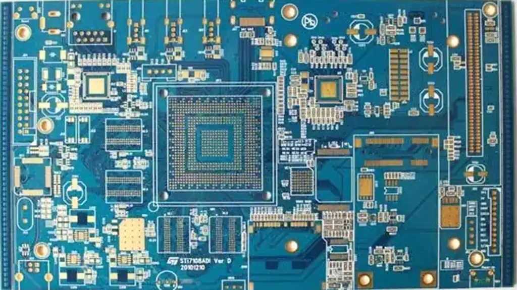
Surface Mount Technology Assembly (SMT Assembly) is an electronic assembly technique in which leadless or short-lead surface-mount devices (SMDs) are directly soldered onto the surface of a printed circuit board (PCB) through processes such as solder paste printing, placement and reflow soldering.
Compared to the traditional DIP (Dual In-Line Package) process, SMT Assembly offers significant advantages in terms of miniaturisation, high density and efficiency. It meets the development requirements of modern electronic products for slimness and integration, and is currently the mainstream assembly process in the electronics manufacturing industry.
Comparison of SMT and DIP Processes
Process Differences: SMT uses surface mounting, where components are placed directly onto the PCB surface without the need for drilling; DIP, on the other hand, requires drilling holes in the PCB, inserting component leads into these holes, and then soldering them in place, making the process relatively cumbersome.
Applications: SMT is suitable for miniaturised, high-density components (such as 0402-packaged resistors and capacitors), is ideal for high-volume production, and is the preferred choice for consumer electronics and AI servers; DIP is suitable for components with longer leads and larger dimensions (such as transformers and connectors), and is well-suited to small-batch, customised production, such as the assembly of high-power components in industrial control equipment.
Cost and Efficiency: SMT requires a higher initial investment in equipment, but offers extremely high efficiency in mass production, with low labour costs per unit; DIP requires a lower initial investment in equipment, but is highly labour-intensive, with low efficiency in mass production, making it suitable for small-batch trial production or custom orders.
Quality Differences: SMT offers high soldering precision, neat component placement and a low failure rate; DIP soldering quality is significantly influenced by manual operation, making it prone to issues such as cold solder joints and false soldering, resulting in higher subsequent rework costs.
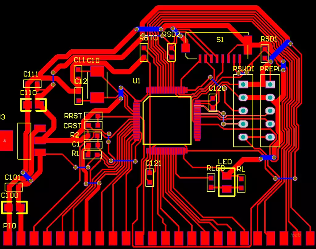
Complete SMT Assembly Process
1.Incoming PCB Inspection and Pre-treatment
This is a fundamental step in SMT assembly, yet one that many manufacturers tend to overlook, which can subsequently affect the quality of the placement and soldering processes.
Practical Guidelines: First, inspect the PCB’s appearance (for damage or warping) and the pads (for oxidation or oil contamination). Use a multimeter to test the PCB’s continuity to ensure there are no quality issues with the incoming materials. During pre-treatment, wipe the pads with anhydrous alcohol to remove oil and dust, thereby facilitating solder paste adhesion.
Recommended Tools: A magnifying glass or AOI (Automated Optical Inspection) equipment can be used for visual inspection; a digital multimeter is required for continuity testing. Smaller manufacturers may opt for a manual magnifying glass, whilst mass production facilities are advised to utilise AOI to enhance inspection efficiency.
2.Solder Paste Printing
This involves evenly applying solder paste to the PCB pads in preparation for subsequent placement and soldering, and is one of the stages in SMT assembly where problems are most likely to arise.
Key Practical Points: Select the appropriate solder paste based on component type and soldering temperature (e.g., high-temperature solder paste with a melting point of 260°C is suitable for high-power components); adjust the stencil thickness (generally 0.12–0.15 mm, depending on pad size) to ensure uniform printing without missed areas or solder bridges; after printing, use a squeegee to level the solder paste, avoiding excess or insufficient paste.
Recommended tools: Semi-automatic solder paste printer (for small manufacturers), fully automatic solder paste printer (for mass production); matching stencil (customised to the PCB layout); solder paste stirrer (to ensure uniformity of the solder paste).
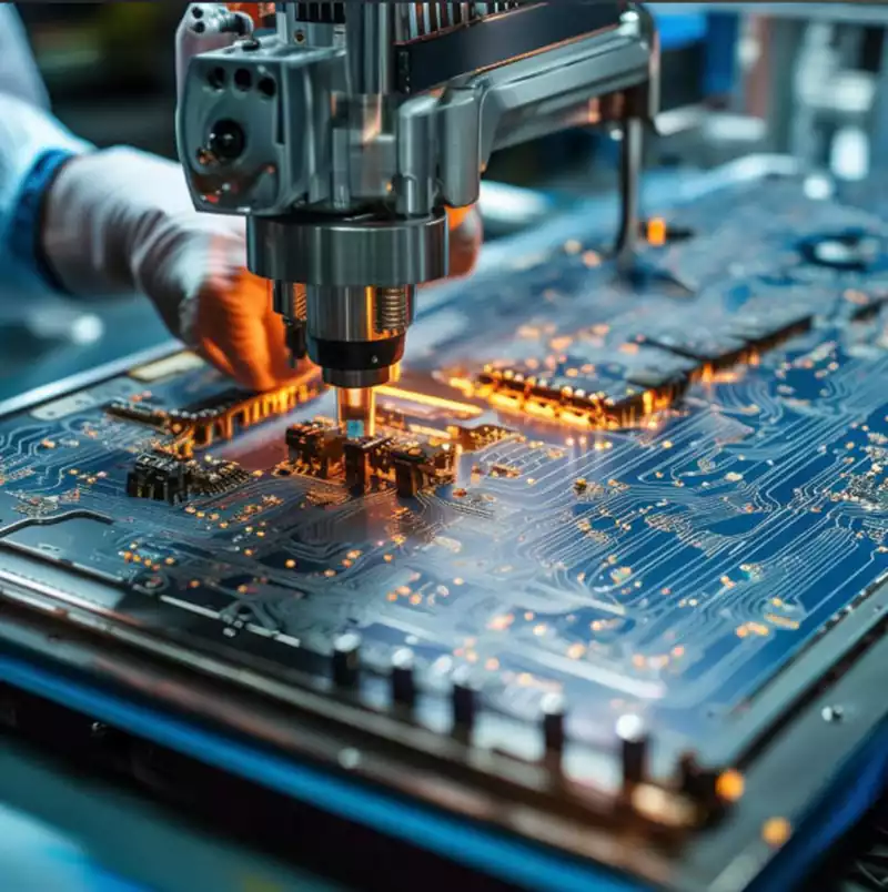
3.Component Placement
SMD components must be placed precisely onto the corresponding pads on the PCB; the key requirements are high precision and zero misalignment.
Key operational points: Select a placement machine according to component type (use a standard placement machine for general components; use a high-precision placement machine for precision components such as BGAs and QFPs; AI robotic placement machines are suitable for high-volume, high-precision production); calibrate the nozzle before placement (to prevent unstable pickup due to wear); set placement parameters (nozzle pressure, placement speed); after placement, check that components are correctly positioned and inspect for misalignment or missed placements.
Recommended tools: General-purpose placement machines (e.g. JUKI, YAMAHA), high-precision placement machines (e.g. FUJI), AI robotic placement machines (suitable for mass production in large factories); placement machine calibration tools.
4.Reflow Soldering
The PCB, with components already mounted, is fed into the reflow oven, where high temperatures melt and then solidify the solder paste, securely bonding the components to the PCB. This is a core step in SMT assembly.
Practical Points: Set a suitable reflow temperature profile (preheating zone 150–180°C, hold zone 180–200°C, soldering zone 240–260°C, cooling zone ≤100°C); different solder pastes require different profiles; control the conveyor belt speed of the reflow oven (generally 1.2–1.5 m/min) to ensure thorough soldering; Inspect the solder joints after soldering to prevent cold joints, false joints and solder bridging.
Recommended tools: Reflow oven (small-scale manufacturers should use a compact reflow oven, whilst large-scale production requires a large tunnel-type reflow oven); temperature profile tester (for temperature calibration).
5.AOI Inspection
Once soldering is complete, conduct a comprehensive inspection of the PCB using AOI equipment to identify soldering and placement defects; this is a critical step in ensuring the quality of SMT assembly.
Key operational points: Set AOI inspection parameters (accuracy, speed) and establish corresponding detection standards for different defect types (cold solder joints, false solder joints, solder bridges, missed components); mark detected defects and hand them over to rework personnel for resolution; calibrate the AOI equipment regularly to ensure detection accuracy.
Recommended Tools: AOI (Automated Optical Inspection) equipment (in-line or off-line; in-line systems are preferred for mass production).
6.Rework and Final Inspection
PCBs with defects detected by AOI are sent for rework. Following repair, a final inspection is conducted to ensure the product meets quality standards.
Practical Guidelines: Select appropriate tools based on the defect type (e.g., use a soldering iron to re-solder for cold solder joints, or a desoldering pump to remove excess solder paste for solder bridges); re-inspect after repair to prevent secondary defects; during final inspection, check the PCB’s appearance and electrical continuity, and proceed to the next stage only after confirming the absence of defects.
Recommended Tools: Soldering iron, desoldering pump, rework station, multimeter.
Common Issues and Troubleshooting in SMT Assembly
Issue 1: Solder Paste Printing Omissions and Solder Bridges
Common Causes: Damaged stencil, insufficient solder paste viscosity, improper squeegee pressure, oil contamination on PCB pads.
Solution: Replace the damaged stencil; stir the solder paste thoroughly (add an appropriate amount of thinner if viscosity is insufficient); adjust the squeegee pressure; pre treat PCB pads to remove grease and dust.
Fault 2: Component placement misalignment or omissions
Common causes: Worn placement nozzle, incorrect placement parameters, faulty component feeder, PCB positioning deviation.
Solutions: Replace worn nozzles; calibrate placement machine parameters (nozzle pressure, placement speed); inspect the feeder; reposition the PCB (adjust the position of the locating pins).
Fault 3: Poor solder joints or cold solder joints
Common causes: Unsuitable reflow soldering temperature profile, poor-quality solder paste, oxidation of PCB pads, oxidation of component leads.
Solutions: Recalibrate the reflow soldering temperature profile; replace with high-quality solder paste; pre-treat pads and leads to remove oxidation; extend the reflow soldering hold time.
Fault 4: PCB Warping
Common causes: Excessively high reflow soldering temperature, poor-quality PCB material, PCB too thin, uneven force applied during soldering.
Solutions: Adjust the reflow soldering temperature profile (reduce the temperature in the soldering zone); select high-quality PCB material (e.g. FR-4); choose an appropriate thickness based on product requirements; use fixtures to secure the PCB during soldering to avoid uneven force.
SMT Assembly Application Scenarios
Consumer Electronics: The field with the widest application of SMT, such as mobile phones, computers and tablets, which require miniaturisation, high density and high efficiency. Fully automated SMT production lines are commonly used, with a focus on placement accuracy and production speed.
AI and Robotics: Examples include AI servers and industrial robots, which demand high precision and reliability. AI-enabled SMT assembly technologies are commonly employed, with a focus on soldering quality and production traceability to prevent equipment malfunctions caused by soldering defects.
Automotive Electronics: Examples include in-car navigation systems and sensors, which require high-temperature resistance and vibration resistance. High-temperature-resistant solder paste and high quality PCBs must be selected, and vibration testing must be conducted post-soldering to ensure stable operation during vehicle use.
Medical Equipment: Such as patient monitors and portable medical devices, which require high reliability and sterility. Production environments must be strictly controlled to prevent contamination, and a comprehensive quality traceability system must be established to meet the compliance requirements of the medical industry.
As a core process in modern electronics manufacturing, SMT assembly offers the advantages of high density, high efficiency and high reliability. From incoming inspection to rework and final inspection, every stage requires meticulous control to effectively address various soldering and placement defects.