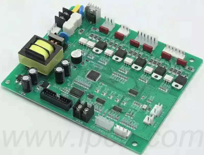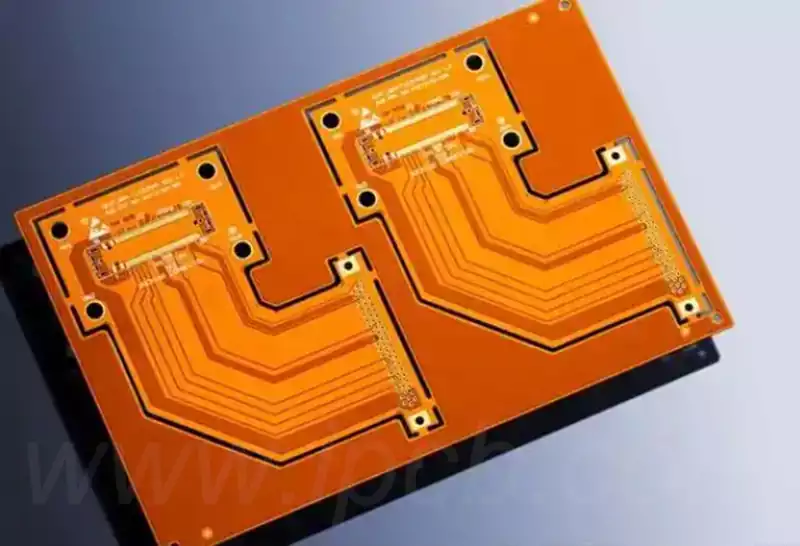
Flexible board vs. rigid pcb and their cost impact factors
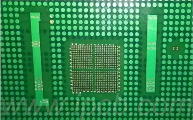
Flexible board, is the so-called flexible circuit board, in fact, also belongs to a kind of printed circuit boards, but with the traditional printed circuit boards and has a great difference, so it will be called flexible board, full name of the flexible circuit board. Flexible board generally use PI as a substrate, is a […]