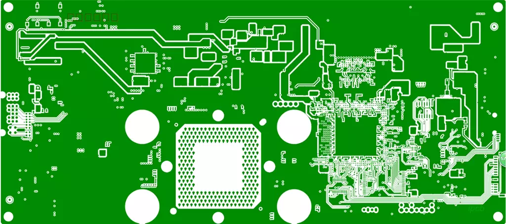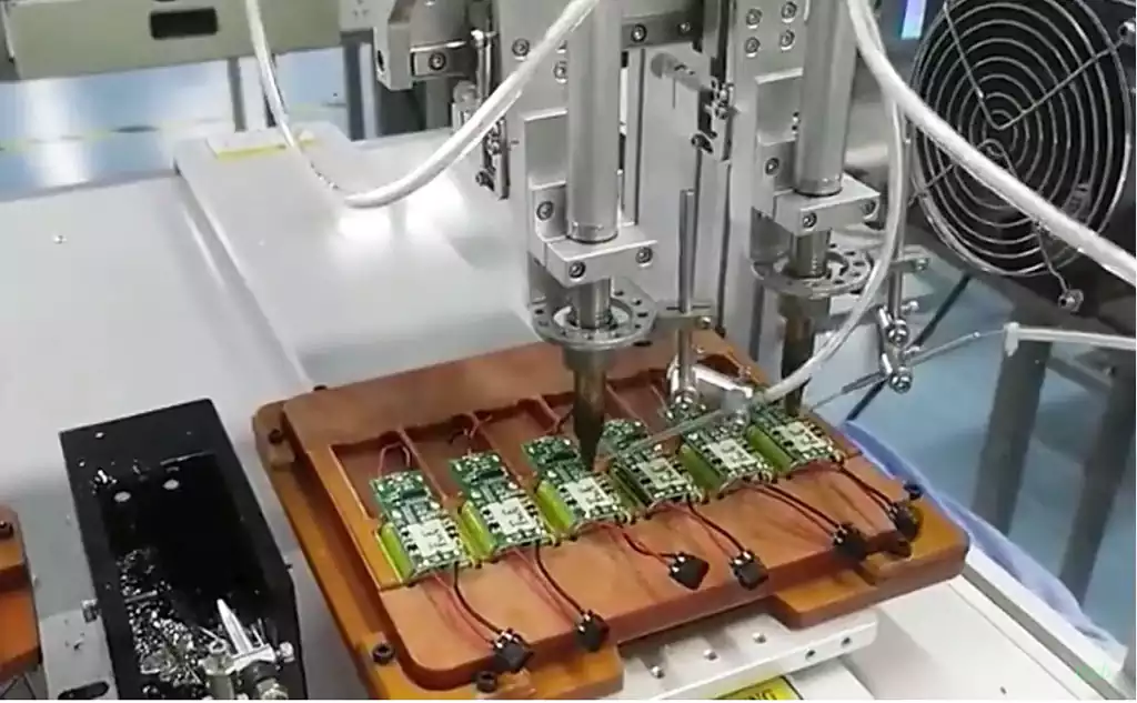
How to clean flux residue is a critical step in soldering
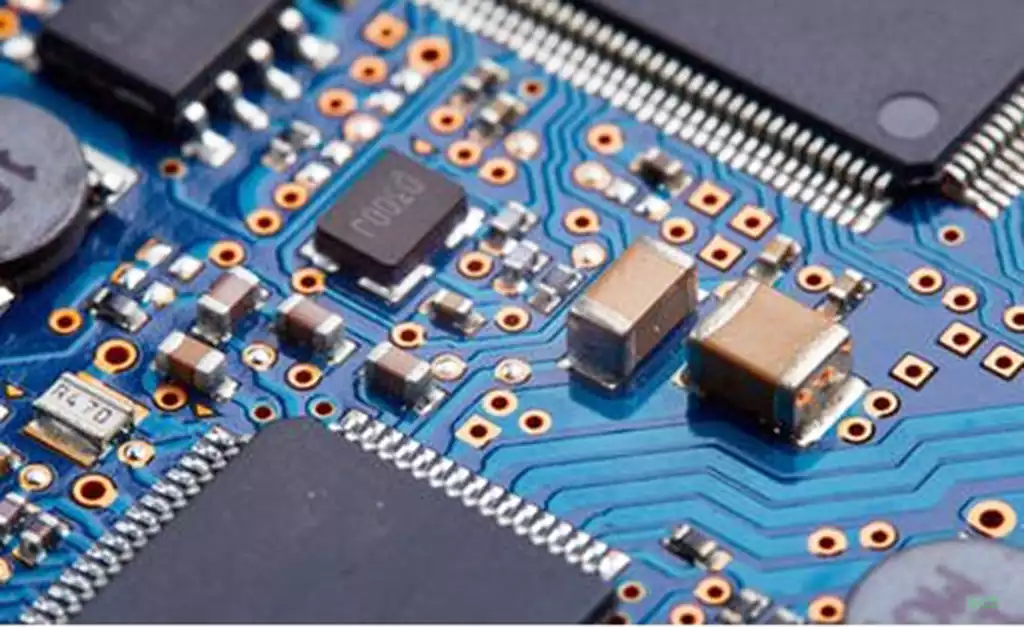
Flux is a chemical substance that removes oxides or other contaminants from the surface of the PCB, the solder itself, wets the metal surface to be soldered, protects the metal surface from re-oxidizing while soldering, reduces the surface tension of the molten solder, and facilitates the expansion and flow of the solder. However, once the […]