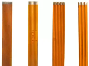
The Role and Challenges of FPC in the 5G Era
What does FPC stand for? FPC stands for Flexible Printed Circuit, known in Chinese as a flexible printed circuit board, commonly abbreviated as a flexible board. FPC is a highly
PCBA Component Spacing Design
Component spacing design on PCBA represents a pivotal aspect of electronic product development, where precision directly influences circuit electrical performance, thermal efficiency, manufacturing feasibility, and the stable operation of the

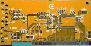
Exposed Copper PCB Trends and Quality in Electronics
Definition and Basic Characteristics In the design and manufacturing of printed circuit boards (PCBs), exposed copper refers to surfaces with exposed copper, not covered by solder or solder mask. Exposed
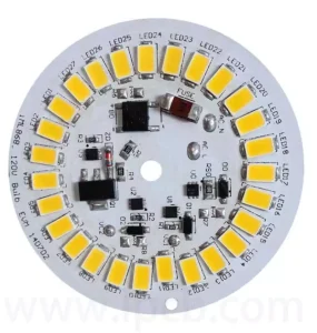
Key Considerations in LED Light PCB Design
LED lighting products’ efficiency, energy-saving properties and extended lifespan have driven their increasing market prevalence. At the core of these products, LED light pcb design is pivotal in ensuring luminaire

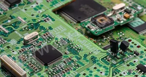
Common PCB Board Defects and Countermeasures
In electronic manufacturing, PCB board quality forms the cornerstone for ensuring device performance and reliability. However, within complex production processes, multiple factors may induce various defects in PCBA, thereby compromising
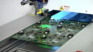
Future of Automated PCB Testing Machine in Smart Electronics Production
Introduction In modern electronics manufacturing, printed circuit boards (PCBs) are considered the “heart” and “nervous system” of electronic products. From smartphones and wearables to automotive electronics, medical devices, and aerospace,
PCB Chamfering Technology Enhances Circuit Board Performance
PCB chamfering, simply put, involves bevelling the edges of printed circuit boards. This process is typically carried out after the boards have been cut, using specialised chamfering machinery or hand
PCBA contaminants and cleaning
The definition of PCBA contaminants refers to any surface deposits, impurities, inclusions, or adsorbed substances that reduce the chemical, physical, or electrical performance of the PCBA to an unacceptable level.
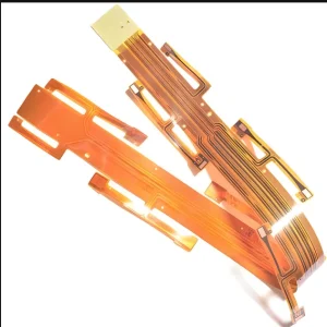
Core Value and Future Development of Etched FPC in Electronics Manufacturing
Introduction In modern electronics manufacturing, flexible printed circuits (FPCs) have become a key technology for connecting miniaturized, high-performance electronic systems. As electronic products continue to evolve toward thinner, smarter, and
PCBA Ion Contamination Testing
PCBA ion contamination refers to residual charged ion contaminants left behind during the manufacturing process of PCBA (Printed Circuit Board Assembly), primarily originating from flux, chemical cleaners, air humidity, electroplating,
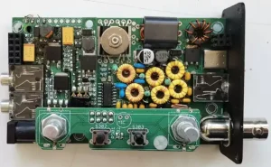
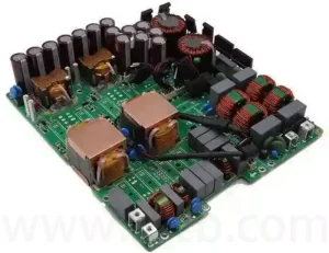
Classification and Design of UPS PCB
UPS PCB, short for uninterruptible power supply printed circuit board, is the core control board of the UPS system. It is primarily responsible for providing emergency power to equipment when
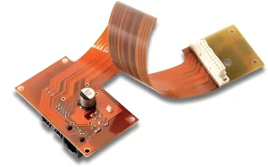
Flex assembly manufacturing process and quality control
Introduction – The Importance of Flex Assembly and Industry Background As electronic products continue to evolve towards thinner, more compact, and higher-performance designs, traditional rigid PCBs are no longer able
Causes and Solutions for False PCB Exposed Copper
After the PCB circuitry is etched, a layer of ink (green ink, blue ink, black ink, etc.) needs to be applied. However, ink is liquid and has flowability. During the
PCB Manufacturing Expenses and Optimization
In today’s highly integrated electronic product era, circuit boards serve as core components, and pcb manufacturing costs directly impact the market competitiveness of the final product. Accurately understanding the composition
What is a presensitized PCB board?
What is a presensitized PCB board?A presensitized pcb board is a special type of printed circuit board with a photosensitive surface. It supports photolithography technology and can be adjusted using
PCB board testing methods and advantages
PCB board serves as the core components of electronic products, and their quality directly impacts the performance and reliability of the final product. With the rapid advancement of electronic technology,
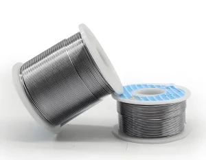
Everything You Need to Know About Soldering Wire
Introduction and Definition of Soldering WireIn modern electronics manufacturing, metalworking, and various electrical assembly processes, soldering is a crucial process for connecting components and conductors. Among the many soldering materials,

Board-level EMI shielding technology in PCB design
EMI radiation consists of electric and magnetic fields, which disrupt the normal operation of electronic devices. These electromagnetic waves propagate within electronic devices and interfere with electrical components, with their
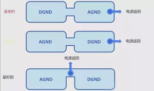
Key Considerations for PCB Grounding Design
The pcb grounding plane on a PCB is typically a large metal area connected to the circuit ground. This metal area may only occupy a small portion of the board
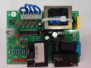
How to Tell if Your Aquarite Control Board is Bad
Introduction – Why Pay Attention to the Health of Your Aquarite Control Board In swimming pool water quality management, automated salt chlorination systems are widely adopted for their efficiency, environmental
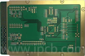
PCB board layer layout principles
A PCB board layer typically refers to the number of conductive layers within a printed circuit board (PCB). These conductive layers are made of copper foil and are a critical
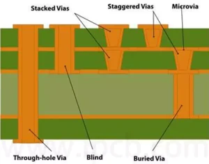
The key role of PCB via plugging
Conductive via holes, also known as through holes, pcb via must be filled to meet customer requirements. After extensive testing, the traditional aluminium plate filling process has been replaced with
Key points in PCB pad design
PCB pad is a critical component of printed circuit boards, serving as the interface between electronic components and the circuit board for establishing electrical connections and mechanical support. The quality
PCB aspect ratio design reference factors
The pcb aspect ratio, which is the ratio of the length to the width of the circuit board, is a critical parameter in electronic design. The aspect ratio refers to