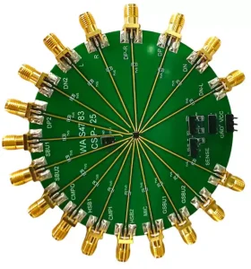
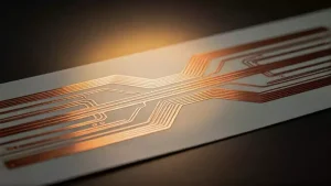
Tips for designing thick copper PCBs
The design of thick copper PCBs differs significantly from that of conventional thin copper PCBs. The core challenge lies in ‘balancing high current-carrying capacity, efficient heat dissipation and manufacturing feasibility’—line
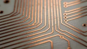
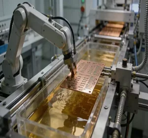
Causes and Control of Undercutting in the PCB Etching Process
Underetching of PCB circuit traces primarily occurs during the etching process. Any deviation in the concentration, temperature, spray pressure or etching time of the etching solution will significantly increase the
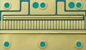
Comparison of Ceramic PCB Manufacturing Processes: Subtractive and Additive Methods
Every improvement in the precision of flexible circuit formation drives the expansion of ceramic pcb into high-end applications such as 5G communications, medical electronics and aerospace. As the two core
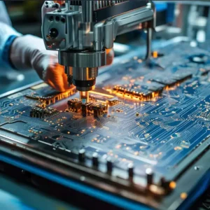
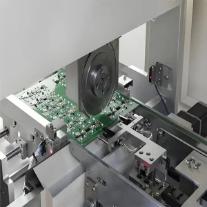
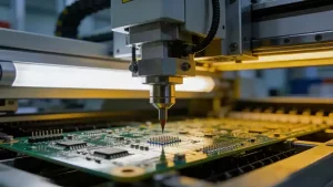
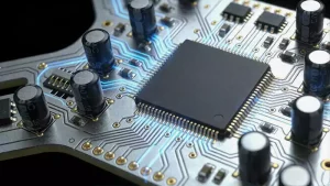
An Analysis of the SMT Assembly Process
Surface Mount Technology Assembly (SMT Assembly) is an electronic assembly technique in which leadless or short-lead surface-mount devices (SMDs) are directly soldered onto the surface of a printed circuit board
High-frequency low-loss FPC material
High-frequency, low-loss FPCs (flexible printed circuit boards) are the key medium for signal transmission in 5G communication equipment; their material properties directly determine the transmission speed, stability and coverage of
A Detailed Guide to Metal Core PCBs(MCPCBs)
Metal Core PCB (MCPCBs), also known as Insulated Metal Substrate (IMS) PCBs or thermal PCBs, are a type of printed circuit board that uses a metal plate as the substrate
Ceramic circuit boards in extreme-duty military sensors
Ceramic circuit boards offer unique advantages in terms of wide temperature ranges, high thermal conductivity, high-frequency stability and resistance to harsh environments, enabling them to meet the stringent requirements of
Key Characteristics and Applications of High Frequency PCB Materials
With the trend towards higher frequencies, miniaturisation and higher performance in electronic devices, high frequency PCBs (printed circuit boards) are now widely used in fields such as 5G communications, satellite
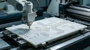
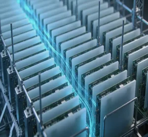
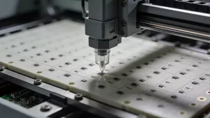
The role of PCB cutting machines in the electronics industry
Industry Challenges, Evolution, and the Historical Framework of PCB Cutting machines Technology About pcb cutting machines, In an era where electronic product iteration cycles are measured in months, the PCB,
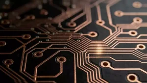
The impact of PCB ink on PCB performance
In the PCB manufacturing process, although pcb inks are classified as auxiliary materials, they play an indispensable role in PCB circuit boards. Different types of ink not only determine the
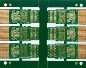
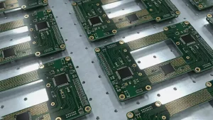
The Breakdown of HDI PCB Costs and Optimisation Strategies
High-Density Interconnect (HDI) PCBs, with their finer line widths, smaller via diameters and higher routing density, have become indispensable core components in sectors such as smartphones, high-end telecommunications equipment and
The Key Role of PTFE PCBs in 5G Base Station Antennas
Against the backdrop of 5G base stations evolving towards millimetre-wave technology, antennas—as key components for signal transmission and reception—directly influence network coverage capabilities. PTFE PCB (polytetrafluoroethylene printed circuit board) is
Key aspects of impedance control in the mSAP process
In the mSAP process, the core of impedance control lies in ensuring that the impedance of PCB traces meets design standards through comprehensive parameter management throughout the entire process. Compared
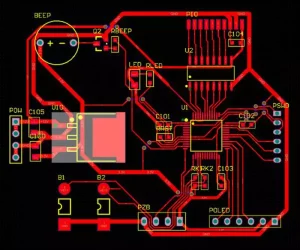
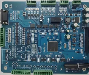
Manufacture of drone flight control boards and their PCBs
The flight control board is the core control unit of a drone, responsible for attitude calculation, sensor fusion and the execution of flight algorithms. Its PCB primarily carries high-speed signals,
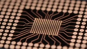
mSAP process technology
mSAP (Modified Semi-Additive Process) is a high-precision manufacturing technology designed for High-Density Interconnect (HDI) PCBs. Its core principle is ‘seed copper plating + selective etching’. By adopting an ‘additive’ approach—the
Common surface treatment processes for FPCs
FPC surface treatment is not merely an optional auxiliary process, but a critical step that determines soldering reliability and storage life. Bare copper is highly susceptible to oxidation; without protection,
Low-dielectric polymer materials and high frequency PCBs for 5G/6G
With 5G moving towards millimetre-wave frequencies and 6G targeting the terahertz range, high-frequency signals place unprecedented demands on PCB substrates to achieve low loss. Low dielectric polymer materials, with their
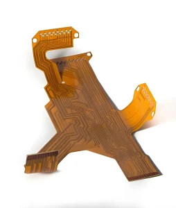
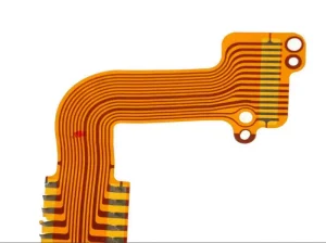
Flex PCB Thickness and Performance in PCB
The Multidimensional Composition of Flex PCB Thickness: Beyond the Definition of “Board Material” When we talk about flex PCB thickness, we are dealing with a dynamic, multi-material composite system. Unlike
Rogers PCBs and Key Technologies for 77 GHz Radar
77GHz radar primarily utilises Frequency-Modulated Continuous Wave (FMCW) technology: by transmitting a linearly frequency-modulated ‘chirp signal’ and analysing the frequency and phase differences between the reflected echo and the transmitted
High Layer PCBs Manufacturing Challenges and Technologies
Compared to conventional printed circuit boards, high layer PCBs are characterised by greater board thickness, a higher number of layers, denser traces and vias, larger component dimensions, and thinner dielectric
Causes of Electromagnetic Interference in Drone PCB Boards and Mitigation Measures
The drone pcb board serves as the core component of the flight system, and its electromagnetic compatibility directly affects the stability of the drone’s flight. In high-frequency operating environments, circuit
Drone PCB board why 4 layer or 6 layer designs are preferred for performance and reliability
In drone pcb board design, the printed circuit board directly impacts signal stability, flight safety and flight endurance. Striking the right balance between performance, cost, weight and reliability is key
SMT Process for Ceramic PCBs
Ceramic PCBs are not merely a simple substitute for FR-4. Thanks to their inherent advantages—such as low thermal expansion, high insulation and high-temperature resistance—they are widely used in demanding applications
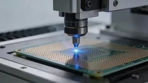
Guidelines for the Prevention and Control of Solder Balls
Solder balls are discrete particles of molten solder that form during the reflow soldering process when the molten solder fails to wet the component leads or PCB pads properly, and