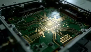
High Frequency Board Technology for 5G Base Stations
In the current era where 5G communication technology is reshaping the global information landscape with lightning speed, 5G base stations, serving as the “nerve endings” of network coverage, directly determine
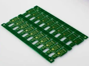
4 layer PCB High-Efficiency Heat Dissipation Design Strategy
In the era where electronic devices are constantly evolving towards higher performance and greater integration, the heat dissipation issue of PCBs has become increasingly critical. Copper, with its outstanding thermal
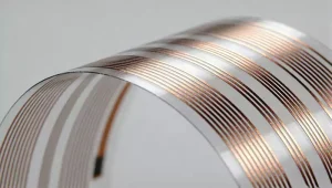
Differences in 4 layer FPC bend design
Flexible Circuit Boards (FPCs), with their unique bendable properties, have become a key component in high-end applications such as foldable smartphones, wearable devices, and industrial robots. Among them, 4-layer FPCs
How does the thickness of PP film affect PCB impedance?
Precise control of interlayer spacing is the true key to achieving stable pcb impedance, and prepreg thickness is the “behind-the-scenes driver” that determines that spacing. How are interlayer spacing and
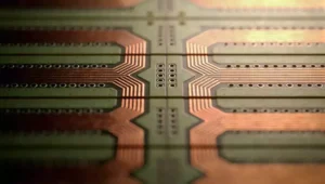
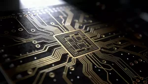
Controlled Impedance Design for FR4 High Speed PCB
For high-frequency or high-speed digital circuits, wiring on FR4 materials is no longer as simple as just connecting components. Impedance-controlled design directly affects signal integrity, electromagnetic compatibility (EMC), and system
Preventing reference plane gap hazards in 4 layer PCB Boards
In a 4 layer PCB board, although signal crossing over reference plane gaps may seem minor, it can trigger a series of issues such as signal distortion, electromagnetic interference (EMI),
Key Considerations for Differential Wiring Switching in 4 layer pcb
When routing differential wiring on 4 layer pcbs, inadvertent interlayer transitions can readily cause signal distortion and a sharp decline in product yield. Unlike single-layer or thick multilayer boards, the
Breaking Through with Ultra-Fine Circuit Design on HDI Boards
In the context of the PCB manufacturing industry’s upgrade towards high-end and miniaturization, HDI boards, with their unique technological architecture, have become the core carrier for solving the challenges of
Causes and Remedies for PCB Pad Detachment
The PCB pad, as a critical part connecting components to the PCB, directly determines the performance and stability of the entire circuit. However, in actual production and maintenance processes, pad
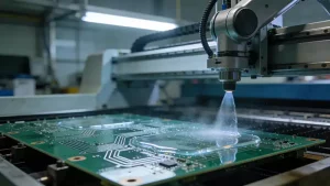
PCB Conformal Coating Application Process
Conformal coating, also known as triple-proof coating, is a functional polymer coating material specifically developed for printed circuit boards (PCBs). Its core function is to form a dense protective film
Inner Layer Black Oxide Process for PCBs
The inner layer black oxide process is one of the earliest surface treatment technologies applied in multilayer PCB manufacturing. With mature technology and relatively low cost, it is still widely
Impedance Boards and Production Tolerance Control
Impedance Boards (commonly referred to as impedance boards) are specialized circuit boards in PCB manufacturing that require precise design, calculation, and strict production control of signal trace characteristic impedance. Their
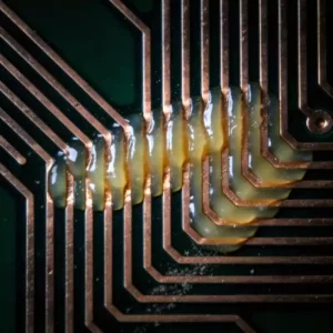
Analysing the Hazards of Flux Residue on PCB
In PCB soldering processes, the role of flux is indispensable. Without high-quality flux, even with premium solder and precision equipment, achieving acceptable solder joints remains challenging. Yet flux exhibits a
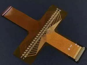
Key Considerations for Material Selection and Routing Design in FPC Design
FPC has gained increasing application in the trend towards miniaturisation and portability of electronic devices, owing to their unique flexibility. However, FPC design is complex and specialised, involving multiple critical
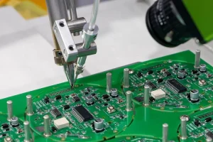
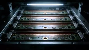
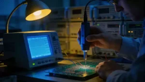
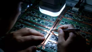
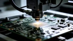
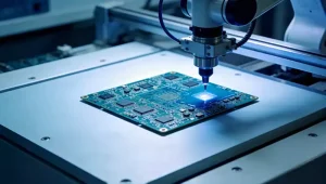
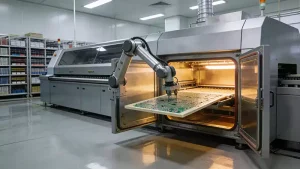
PCB Board Soldering Machine: Ensuring Consistent and Reliable Assembly
The Core Role of PCB Board Soldering Machines in Electronics Manufacturing In the electronics manufacturing process, PCB board soldering machines are one of the key links determining product reliability and
Optimising control loop area within the inner layers of 4 layer board
PCB loop area refers to the physical spatial area enclosed by the closed circuit formed by current flow on a printed circuit board (PCB). It is a critical factor influencing
The Impact of 4 Layer Board Via Parasitic Parameters on Signals and Optimisation Strategies
In 4 layer board designs (typical stack-ups such as signal layer-ground layer-power layer-signal layer), vias serve as the core carriers for interlayer interconnections, facilitating signal, power, and ground continuity between
Causes and Hazards of Warpage in 4 Layer PCBs
In actual production and usage, warping issues in 4 layer PCBs are frequently encountered. This not only impacts production yield and assembly efficiency but also poses long-term reliability risks for
The role of the core board and prepreg in a 4-layer PCB
4-layer PCBs find extensive application across numerous sectors including consumer electronics, industrial control systems, and automotive electronics. Their pivotal role owes much to the core materials—the core board and prepreg.
Moisture Resistance of FR4 PCBs
The moisture resistance of FR4 PCBs is directly linked to the stability and longevity of electronic products. Material selection, process optimization, and strict environmental control are all indispensable. Only through
Reflow Soldering Temperature Profile for Ceramic Circuit Boards
Ceramic circuit boards, owing to their high-temperature resistance and superior thermal conductivity, have progressively become the preferred substrate for high-power electronic components. However, their inherent ceramic properties pose significant challenges
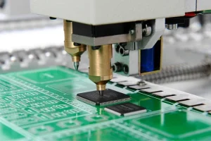
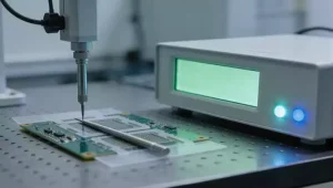
Why Prototype SMT Assembly Determines Manufacturing Success
The Core Value and Industry Positioning of Prototype SMT Assembly In today’s world of increasingly compressed electronic product development cycles, Prototype SMT Assembly is no longer just a simple step
Aluminium nitride ceramic circuit boards empower laser diode applications
Behind the faint light pulses of laser diodes lies an uncompromising demand for substrate material. From the precise detection of autonomous driving lidar to the high-speed transmission of 800G optical
Thermal Conductivity Properties and Development Trends of Ceramic Circuit Boards
When the thermal conductivity of conventional FR-4 substrates, typically below 1 W/(m·K), proves inadequate for managing the thermal loads of high-power devices, ceramic circuit boards emerge as the preferred solution.