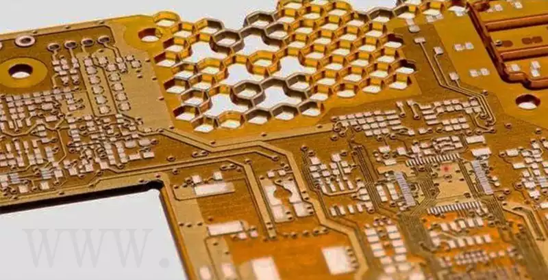
3D printed pcb boards are spearheading a disruptive transformation in manufacturing processes. Unlike traditional fabrication methods—which commence with copper-clad laminates and progressively remove excess material through subtractive techniques such as chemical etching—3D printing employs an additive approach, building circuits layer by layer from scratch. This shift not only reconfigures PCB production logic but also signifies a paradigm leap in electronics manufacturing—from a ‘subtractive mindset’ to ‘additive innovation’.
The core advantage of 3D printed PCB boards lies in their astonishing speed for prototyping. Processes that might take days or even weeks for traditional manufacturers can now be completed in a matter of hours on a desktop. This acceleration enables rapid iteration: circuit design, printing, testing, and optimisation can be accomplished within a single day. For hobbyists, researchers, and engineers requiring swift, efficient design validation, this represents a transformative breakthrough.
Beyond speed advantages, 3D printing significantly reduces costs while offering design freedom. For single prototypes or small-batch production, you avoid the steep setup fees and minimum order quantity constraints of professional services, making exploration of new ideas accessible. It also breaks free from the limitations of flat, rectangular circuit boards. Additive manufacturing enables routing on curved surfaces, flexible substrates, and complex three-dimensional structures, opening new possibilities for integrated electronics in wearables, custom enclosures, and more.
This technology particularly empowers makers and small-scale developers. By integrating PCB manufacturing into in-house processes, you gain complete control over the supply chain, eliminating shipping delays or external production queues. While this technology may not match mass-produced circuit boards in conductivity or scalability, its value in manufacturing customised, small-batch, geometrically complex circuits is undeniable.
Multiple innovative approaches exist for repurposing 3D printers as PCB fabrication equipment, each offering distinct application scenarios, technical advantages, and implementation challenges. Selecting a solution tailored to the requirements of specific electronic projects and the technical proficiency of the maker can significantly enhance production efficiency and final product quality. Below is an in-depth analysis of three mainstream methods:
Method One: Dual-Material Direct Printing
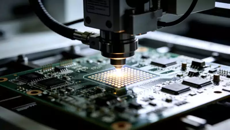
The most straightforward solution involves using a dual-extruder 3D printer to achieve end-to-end PCB manufacturing. This technology employs dual nozzles working in tandem: one deposits a non-conductive substrate (such as PLA or ABS) to form the PCB’s base structure, while the other simultaneously lays conductive composite material (e.g., silver-based or copper-based filament) to create the circuit traces. As demonstrated in tutorials published on the Instructables platform, this method enables the one-step production of 3D solid circuits featuring embedded traces, vias, and multi-layer structures. Key implementation considerations include: precise dual-extruder alignment calibration (with tolerances within ±0.05mm), optimising adhesion strength between conductive materials and substrates, and specialised component mounting techniques—employing conductive adhesives or cold soldering instead of conventional soldering to prevent high-temperature degradation of the plastic substrate.
Method Two: Printer Functionality Expansion: Dual Etching/Milling Mode
Modular retrofitting to upgrade standard 3D printers into 2.5-axis machining equipment offers another cost-effective solution. Two technical pathways exist for this modification:
Chemical Etching Path: Replace the print head with a high-precision marker pen or conductive pen to draw resist patterns on the copper-clad laminate surface. Subsequently, selectively remove exposed copper layers via chemical etching processes (e.g., immersion in ferric chloride solution). Practical guides on Instructables indicate this approach requires addressing pen tip pressure control (pneumatic drawing pens are recommended) and pattern accuracy compensation algorithms.
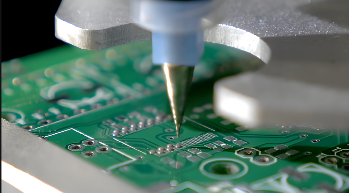
Mechanical milling approach: Install miniature rotary cutters or engraving heads to convert the device into a lightweight CNC milling machine. Control tool paths via G-code to physically remove excess copper foil. This method demands high rigidity (recommended metal-reinforced frame) but entirely avoids chemical waste disposal, making it suitable for simple single-sided or double-sided boards.
Method Three: SLA Photopolymerisation-Assisted Lithography
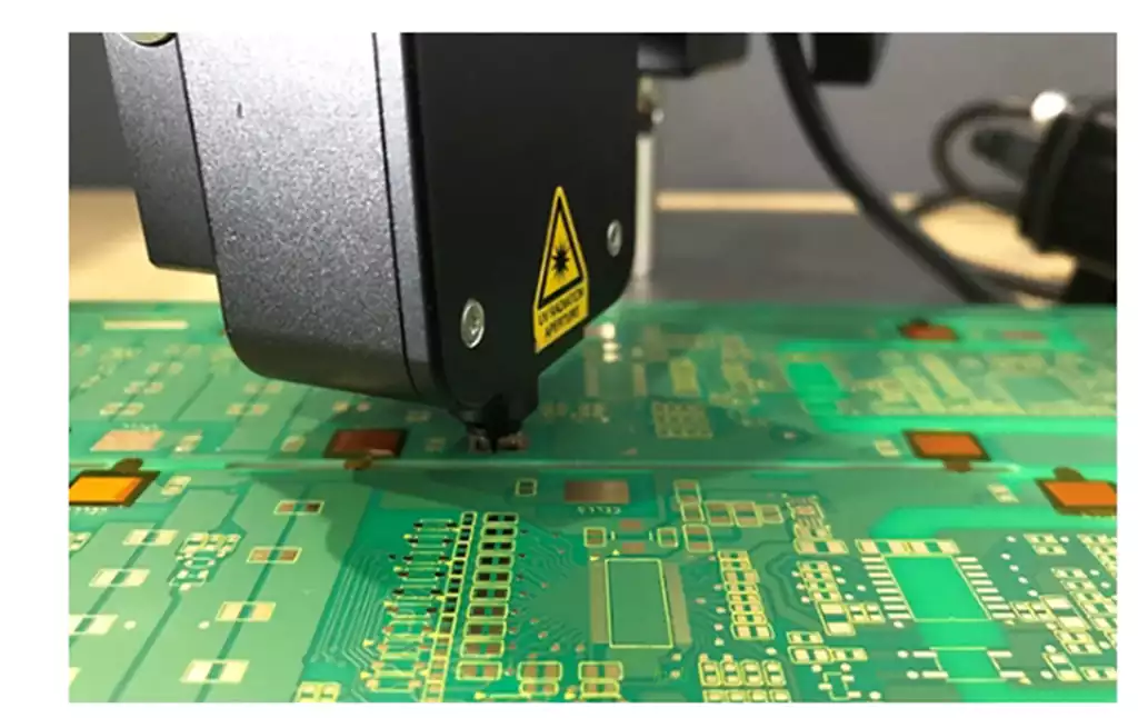
For high-precision applications, the ultraviolet light source system of a stereolithography (SLA) printer enables nanoscale circuit fabrication. The process involves uniformly coating the copper-clad laminate surface with a photosensitive resist, then utilising a modified SLA device (with the resin tank removed) as an ultraviolet exposure unit. Programmed control of the laser or DLP grating projects the circuit design onto the board surface, achieving selective curing. Following development processing, uncured areas are washed away, forming a precise etching mask. Leveraging the SLA equipment’s positioning accuracy of up to 20μm, this technique enables intricate circuits with line widths/spacing of 0.1mm, rivalling industrial-grade photolithography processes. Key implementation considerations include: uniformity control of photosensitive coating thickness (rotary coating recommended) and UV wavelength matching (requiring a 365nm light source).
In-depth Comparison Between 3D Printing and Traditional PCB Manufacturing
The choice between 3D printing and conventional PCB manufacturing hinges entirely on project objectives. 3D printing excels in prototyping through speed and flexibility, while traditional methods remain unrivalled in volume production for scalability and precision. The fundamental distinction lies in their process nature: 3D printing employs additive manufacturing to build circuits layer by layer, whereas traditional methods utilise subtractive processes to etch circuits from solid copper plates.
For hobbyists or small R&D teams, the ability to produce functional circuit boards within hours offers significant advantages. This on-demand production capability eliminates waiting for manufacturer shipments, enabling immediate design testing and validation, thereby substantially shortening development cycles. However, materials such as conductive filaments used in direct 3D printing exhibit higher electrical resistance than pure copper, potentially limiting their suitability for high-power or high-frequency circuits.
Conventional manufacturing, conversely, is optimised for mass-producing thousands of highly reliable, identical circuit boards. Its standardised materials (e.g., FR-4 substrates) and processes yield circuits with exceptional electrical performance and durability. While unit costs are extremely low in high-volume production, initial setup costs and minimum order quantity restrictions make it difficult to meet single-unit prototyping demands. It is precisely in this context that 3D printing technology fills a critical gap in the electronics development process.
Application Scenarios:
- Rapid Prototyping and Small-Batch Customisation
In high-iteration fields such as drones and robotics, 3D printed PCB boards reduce R&D cycles from weeks to hours. A drone manufacturer reduced prototyping costs for custom-shaped circuit boards by 70% through 3D printing, while achieving integrated antenna-structural designs that cut weight by 15%. Educational institutions similarly benefit: university electronics labs employing desktop 3D printers enable students to validate course designs within a single day, bypassing the high barriers of traditional methods. - Advanced Medical and Bioelectronics
3D printed flexible circuit boards are reshaping medical electronics. For instance, a team’s brain-computer interface device features conductive circuits directly printed onto a silicone substrate, achieving a mere 0.3mm thickness for seamless integration with cerebral cortex. Another implantable sensor employs a biocompatible resin-printed casing housing an internally integrated 3D-printed microelectrode array, enabling long-term monitoring without rejection reactions. - Extreme Environments and Specialised Equipment
Within aerospace, the lightweight advantages of 3D printed PCB boards are particularly pronounced. A satellite project utilised titanium alloy substrates with carbon nanotube conductive pathways, reducing antenna module weight by 40% while withstanding temperatures ranging from -150°C to 120°C. Within military applications, the rapid repair capabilities of 3D printing enable on-site replacement of damaged circuit modules, compressing maintenance time from days to just two hours.
As 3D printing technology breaks free from the constraints of traditional processes, electronics manufacturing is transitioning from standardised production to a new era of personalised creation. Whether accelerating innovation through rapid prototyping or pioneering specialised applications in extreme environments, this technology is redefining the boundaries of what is possible. With ongoing breakthroughs in materials science and intelligent algorithms, 3D printed PCB boards will ultimately propel the electronics industry into a new manufacturing era characterised by greater freedom, agility, and sustainability.