The design layout of a camera pcb board is a central aspect of ensuring camera performance, reliability and stability. An optimised layout can effectively reduce signal interference, improve signal integrity, and improve thermal management.
Camera PCB Board Wiring Guide
The LVCMOS signal alignment needs to be away from the differential lines to prevent the LVCMOS line signals from coupling to the differential lines.
Video transmission high-speed signal lines have the highest priority in isometric control . Impedance matching and other key control points need to be prioritised to meet the cabling requirements.
CLK and DATA need to be strictly equal in length and the impedance should be consistent.
In order to reduce crosstalk and reflections between channels, the spacing between each differential channel should be at least three times the width of the cabling. Also minimise the number of vias in the routing path, ideally two or less to minimise stubs and reduce reflections.
The number of left and right bends in the alignment should be as equal as possible, and the angle of the bends should be greater than or equal to 135 degrees.
High-frequency decoupling capacitors with small capacity should be placed as close to the device as possible, and the decoupling capacitors should be placed in consideration of the return path to reduce parasitic inductance as much as possible.
Coaxial cable transmission line impedance control for 50 Ω, as indicated by the yellow line in the following figure, as far as possible in the wiring to make the 50 Ω alignment distance shortened.
Camera PCB Board notes for MIPI CSI RX design:
- The decoupling capacitors of all power supplies of Camera shall not be deleted, but must be retained and placed close to the seat;
- Camera’s Reset signal is recommended to use GPIO control, Reset signal of the 100nF capacitance must not be deleted, placed close to the seat, to strengthen the anti-static ability;
- Camera’s CLK clock line should be wrapped with ground processing, wrapped with ground alignment every 300mil to add GND holes, if the space is not recommended and he went down to pull away at least 3W spacing.

Camera PCB Board Core Design Essentials
The design layout of a camera pcb board requires comprehensive consideration of several aspects to ensure circuit performance and reliability.
Wiring Order and Partitioning
Priority: In mobile phone PCB layout, the wiring order is critical and usually follows the principle of going from Radio Frequency (RF) to Analog, then Digital, and finally Power. This order helps to avoid crosstalk and interference between signals.
Modular Partitioning: Modular partitioning is recommended to minimise interference by laying out high frequency signals, digital circuits, analogue circuits and power supply sections separately.
Critical Signal Priority: Critical signal lines should be prioritised and their paths kept as short and straight as possible, especially for RF signals and high speed signals, to reduce signal delay and crosstalk.
Signal Integrity
Differential Signal Cabling: For high-speed differential signals such as MIPI, differential routing and impedance control are necessary to ensure signal integrity. At the connector, adjacent differential signal pairs should be isolated from each other using the GND (ground) pin. If perforated isolation is not possible, the spacing between differential pairs should be maintained at least 15 mils, and the entire differential signal should be ground-packed.
Impedance Control: Since camera PCB board transmits high frequency signals, impedance control is very important in the design, manufacturing and performance phases. Accurately matching alignment impedance is critical to maintaining signal clarity and data integrity.
Reduced Signal Paths: All signal line connections between the image sensor and the FPGA (Field Programmable Gate Array) should be directly connected, avoiding additional inter-board connectors, to reduce signal transmission paths and improve signal quality and reliability.
Filter Capacitors: All power supply decoupling capacitors of Camera must be retained and placed close to the sockets. a large number of filter capacitors of the FPGA control chip should be reasonably laid out in the leakage area of the sensor sockets according to the actual height in order to ensure the signal quality of the FPGAs and to reasonably utilise the board area.
Power and Ground
Power Decoupling: All decoupling capacitors of Camera power supply must be kept and placed close to the sockets.
Power Wiring: Analogue and digital power supplies should be wired separately for each layer to avoid crosstalk. The three power supply currents must pass through the capacitors before reaching the power pins of the chip. For example, AVDD requires a separate external 2.8V power supply and three capacitors (22uF+0.1uF+10nF) placed near the pins of each power supply to the chip.
Ground plane: EMI/EMC (Electromagnetic Interference/Electromagnetic Compatibility) can be effectively suppressed by using ground planes, shielding cases and electromagnetic filters.
Thermal Management
Heat Source Dispersion: High power components should be dispersed as much as possible to avoid concentrated heat sources.
Heat Dissipation Measures: Thermal vias, copper blocks, graphite sheets, or metal heat sinks can be used to cool down the heat source. Highly heated components are recommended to be wired independently and away from the sensor area.
Component Arrangement: Components of different sizes should be arranged as evenly as possible to ensure even wind resistance and airflow distribution.
Space Optimisation and Component Layout
Key Component Locations: Sensors, ISP chips and filter capacitors should be arranged as close as possible to reduce signal delay.
Miniaturisation: Optimising the image sensor and FPGA controller on the same board reduces board size and eliminates connector area. By using the image sensor socket with a BGA package and an empty space in the middle, the filter capacitors of the FPGA controller can be placed in the empty area, thus making rational use of the board area and facilitating the replacement of the image sensor.
Size and Mechanics: Module size is usually limited by the phone’s notch or lens module housing. Keeping the optical axis of the lens precisely aligned with the centre of the sensor is key to ensuring image quality.
Design Flow
Schematic and PCB Layout Interaction: During the design process, there should be effective interaction between the schematic and PCB layout to ensure consistency and correctness of the design.
Component spacing specifications: Following IPC (International Powered Connectivity) component spacing specifications can help create camera PCBs that reduce interference and optimise space utilisation. for example, IPC-2221 and IPC-7251 provide detailed specifications for through-hole design, including positional tolerances, minimum ring sizes and pad requirements.
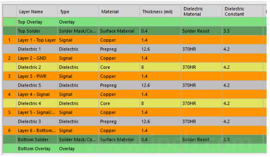
PCB stacking design car camera PCB board design needs to take into account the car regulations for the ambient temperature, vibration, service life, complex electromagnetic environment requirements, comprehensive consideration of a variety of extreme use scenarios, in order to meet the product’s performance and dimensional requirements under the conditions of the selection of the board and the corresponding stacking programme.
The programme requires at least four layers of boards with power and ground layers. If a four-layer board design is used, the second layer must be the ground layer. Since most of the switching devices are located on the top layer, this design minimises stray inductance from through holes in the return path.
To simplify BGA fan-out and wiring difficulties, the solution uses a 6-layer board for the stacked design.